
 E-mail Alert
 RSS
RSS
-
摘要
双曲超材料作为电磁超材料的重要分支,因其独特的近场调控特性成为研究的焦点。双曲超表面作为一种特殊新型的平面超材料,具有双曲色散特性,在理论和应用上也与双曲超材料有诸多相似点。与块体双曲超材料相比,由于纵向维度尺寸的大幅度减小从而将电磁波传播限制在二维平面上,双曲超表面表现出更加优异的性能。本文首先介绍双曲超材料的理论、实现和应用,接着介绍双曲超表面及其潜在应用,最后还指出双曲超材料和超表面在真实条件下的局限,及对应用前景作了展望。
Abstract
Abstract:As an important branch of electromagnetic metamaterials, hyperbolic metamaterials become the focus of research for their unique property of controlling near-field waves. Hyperbolic metasurface is a new type of planar metamaterials with hyperbolic dispersion relationship and has many similarities in theory and applications with hyperbolic metamaterial. Compared with the bulk hyperbolic metamaterials, hyperbolic metasurfaces exhibit more excellent performances because the large reduction in the longitudinal dimension limits the propagation of the electromagnetic waves in the two-dimensional plane. In the first part of this review, we introduce hyperbolic metamaterial with its theory, implementation and applications. The latter part of the review is about hyperbolic metasurfaces and their potential applications. We also point out the restrictions of the hyperbolic metamaterials and metasurfaces and the prospect of future applications.
-
Key words:
- hyperbolic metamaterials /
- hyperbolic metasurfaces /
- negative refraction /
- hyperlens
-
Overview
In recent years, with the continuous progress of micro/nano fabrication technique, the interaction of material and electromagnetic wave in the subwavelength scale has attracted widespread attention. Electromagnetic metamaterial is artificial material composed of building blocks whose feature size is much smaller than the working wavelength, with the electromagnetic properties that does not exist in natural materials. As an important branch of electromagnetic metamaterials, hyperbolic metamaterials become the focus of research for their unique characteristic to control near-field waves. By changing the size and arrangement of the components of hyperbolic metamaterials, the excitation intensity and direction of the surface plasmons (SPs) in them can be modulated, so that the unique dispersion curves can be achieved. Hyperbolic metamaterials have been used in many fields, such as subwavelength imaging, light localization and enhanced spontaneous emission. Hyperbolic metasurface is a new type of planar metamaterials with hyperbolic dispersion relationship and has many similarities in theory and applications with hyperbolic metamaterial. Compared with the bulk hyperbolic matematerials, hyperbolic metasurfaces exhibit more excellent performances because the large reduction in the longitudinal dimension limits the propagation of the electromagnetic waves in the two-dimensional plane.
In this review, starting with hyperbolic metamaterials, we introduce their basic theory of dispersion equation and isofrequency surface, and then describe the method of realizing hyperbolic dispersion from two different structures: metal-dielectric multilayer structure and metal nanowire structure. Effective medium theory to calculate the effective dielectric tensor and the choice of real materials are also presented. At the end of this section, we briefly introduce the typical applications of hyperbolic metamaterials, including optical negative refraction and hyperlens imaging. The latter part of the review is about hyperbolic metasurface and we begin with the introduction of the basic theory and isofrequency curve of hyperbolic metasurface. The difference is that in addition to the introduction of ordinary hyperbolic dispersion, we also stress the special case of near the topological transition point, where the dispersion curve is almost flat and the transmission of electromagnetic wave is almost diffraction-free. Then we list the natural hyperbolic materials that can be used to fabricate hyperbolic metasurface, including uniaxial and two-dimensional materials. The artificial method of using graphene to achieve any topological structure on the plane is illustrated. In analogy with the hyperbolic metamaterial, the negative refraction effect and the hyperlens imaging in hyperbolic metasurface are also introduced. In addition, intriguing properties of hyperbolic metasurfaces and their potential applications are described. Finally, we point out the restrictions of the hyperbolic metamaterials and metasurfaces and the prospect of future applications.
-
1. 引言
近年来,随着微纳加工技术的不断进步,在亚波长尺度下物质与电磁波的相互作用引起了人们的广泛关注。电磁超构材料是一种由特征尺寸远小于工作波长的结构单元所组成,具有自然界材料所不存在的电磁特性的人工材料[1-4]。作为电磁超构材料的一个重要分支,双曲超材料由于其独特的近场电磁波操控特性成为人们研究的焦点。通过改变组成双曲超材料结构单元的尺寸、排布规律,能实现对双曲超材料内部表面等离子体激元激发强度和方向的调控[5],从而使双曲超材料呈现独特的色散特性。双曲超材料已经在很多领域得到应用,包括亚波长成像[6-9]、光场局域[10]和增强自发辐射[11]等。另一方面,双曲超表面作为一种特殊新型的平面超材料,具有双曲色散特性,在理论和应用上也与双曲超材料有着诸多共性。与块体结构的双曲超材料相比,由于其纵向维度尺寸的大幅度减小,双曲超表面可以将电磁波传播限制在二维平面上,非常易于片上器件的集成,因而在近些年受到了研究人员的极大关注[12]。
本文将从双曲超材料出发,首先介绍其色散理论、两种不同类型的超材料和典型应用,再将双曲超表面与之类比,对平面上的双曲效应及典型应用进行介绍。
2. 双曲超材料
2.1 双曲超材料色散理论
众所周知,各向异性材料的介电常数ε为一张量(这里不考虑磁性材料),通过对角化,其在笛卡尔坐标系中可以表示为
\mathit{\boldsymbol{\varepsilon }} = \left[{\begin{array}{*{20}{c}} {{\varepsilon _{xx}}}&0&0\\ 0&{{\varepsilon _{yy}}}&0\\ 0&0&{{\varepsilon _{zz}}} \end{array}} \right], (1) 其中:当 {\varepsilon _{xx}} \ne {\varepsilon _{yy}} \ne {\varepsilon _{zz}} 时,称为双轴材料;当{\varepsilon _{xx}} = {\varepsilon _{yy}} \ne {\varepsilon _{zz}} 时,称为单轴材料;当 {\varepsilon _{xx}} = {\varepsilon _{yy}} = {\varepsilon _{zz}} 时,材料则退化为各向同性。
双曲超材料属于第二种情况的单轴材料,将式(1)代入麦克斯韦方程组,可以推导得出双曲超材料的色散关系为
(k_ \bot ^2 + k_z^2-{\varepsilon _ \bot }k_0^2)\left( {\frac{{k_ \bot ^2}}{{{\varepsilon _{zz}}}} + \frac{{k_z^2}}{{{\varepsilon _ \bot }}}-k_0^2} \right) = 0, (2) 其中: {k_0} = \omega /c 为真空中波矢大小,c为真空中光速, {k_x}, {k_y}, {k_z} 分别为x,y,z方向的波矢。这里假设光轴沿z方向,{\varepsilon _{xx}} = {\varepsilon _{yy}} \equiv {\varepsilon _ \bot } 表示垂直于光轴,并且 {k_ \bot } = \sqrt {k_x^2 + k_y^2} 。当式(2)中的第一项为0时,传播常数与 {\varepsilon _{zz}} 无关,材料中的电磁波被定义为横电波[6];当第二项为0时,传播常数同时与{\varepsilon _{zz}} 和 {\varepsilon _ \bot } 均有关,材料中电磁波被定义为横磁波,此时,其色散方程可描述为
\frac{{k_ \bot ^2}}{{{\varepsilon _{zz}}}} + \frac{{k_z^2}}{{{\varepsilon _ \bot }}} = k_0^2, (3) 当式(3)中的 {\varepsilon _ \bot } 与 {\varepsilon _{zz}} 符号相反时,材料中电磁场的等频面为双曲面,如图 1所示[13]。其中图 1(a)为 {\varepsilon _ \bot } > 0 , {\varepsilon _{zz}} < 0 ,图 1(b)为 {\varepsilon _ \bot } < 0 , {\varepsilon _{zz}} > 0 ,它们分别对应两种不同类型的双曲超材料。相比于各向同性材料,在理想情况下双曲色散材料能够支持倏逝波向前传播,群速度的方向沿着色散等频线的法线方向,这使得材料具有独特的电磁波传播特性;另外,它的双曲线型也会在超材料和普通材料界面形成反常的折射特性。基于这些特性,双曲超材料为一些具有特殊功能的结构器件设计提供了新的思路。
2.2 双曲超材料的构成
自然界中有少量的天然双曲材料,但是这些天然材料呈现双曲色散特性的频率多在远红外和太赫兹频段,因而无法用于可见或紫外频段的器件设计。然而,人们发现通过在亚波长尺度上电磁结构的有序设计,可以实现光频段的人工双曲超材料,但需要满足一定条件——材料的光轴方向和垂直光轴方向的介电函数分量符号相反。对此,前人做了大量尝试工作,发现了满足双曲色散方程的两种典型结构:金属-介质多层膜结构[7, 14-15]和金属纳米线阵列结构[16-18]。
2.2.1 金属-介质多层膜结构
图 2(a)为金属-介质多层膜结构的示意图,图中εi、μi、di(其中i=1, 2)分别代表材料的介电常数、磁导率和薄膜厚度。它由一定厚度的金属、介质薄膜堆叠而成,其中金属、介质层的厚度都远小于入射光波长。根据有效介质理论[19],金属介质多层膜可以从宏观上用有效介电常数表征。Wood等人在前人的基础上利用传输矩阵法计算出这种结构的介电常数分量[20]:
 Figure 2. (a) Schematic of the metal-dielectric multilayer structure, ε, μ, d represent the permittivity, permeability and film thickness respectively [20]. (b) The real part of the permittivity of a semiconductor multilayer structure, ε⊥, ε|| represent the permittivity that are perpendicular and parallel to the film, respectively [15]. (c) Schematic diagram of the nanowire array structure, d is the period of the nanowire array and r is the radius of the metal nanowire [16].
{\varepsilon _{xx}} = {\varepsilon _{yy}} = {\varepsilon _ \bot } = \frac{{{\varepsilon _1} + \eta {\varepsilon _2}}}{{1 + \eta }}, (4) \frac{1}{{{\varepsilon _{zz}}}} = \frac{1}{{1 + \eta }}\left( {\frac{1}{{{\varepsilon _1}}} + \frac{\eta }{{{\varepsilon _2}}}} \right), (5) 其中:η为金属介质薄膜的厚度比, \eta = {d_2}/{d_1} 。当入射光波长的频率小于等离子体频率时,金属材料的介电常数实部为负值,而介质为正值,因此可以通过选择合适的材料,精确地调控膜厚参数和频率范围,从而使得式(4)和式(5)同时满足条件 {\varepsilon _ \bot }{\varepsilon _{zz}} < 0 ,如图 2(b)中的黄色区域所示,最终实现双曲超材料的设计。图中 {\varepsilon _ \bot } , {\varepsilon _{||}} 分别表示垂直和平行于多层膜的介电常数。
通过利用金属介质多层膜结构已经设计了多种双曲超材料。Ferrari等人总结了利用金属介质多层膜结构在实验中已经实现的双曲超材料的结构设计[21],例如在紫外波段的金属介质多层膜有Ag/Al2O3等[7];在可见波段的有Au/Al2O3[22-26]、Ag/PMMA[27]、Al/MgF2[27-28]、Ag/TiO2[29]等;在红外波段的有AlInAs/InGaAs[15]、Al:ZnO/ZnO[30]、Ag/Ge[31]等。另外,值得一提的是,在选材和结构参数设计时,除了要满足双曲条件,还需注意损耗和阻抗匹配的问题。
2.2.2 金属纳米线阵列结构
图 2(c)为金属纳米线阵列结构示意图,图中d为金属纳米线阵列周期,r为金属纳米线半径。它通过将金属纳米线阵列嵌入介质中构成。同样,金属纳米线阵列的周期远小于波长时,也可用等效介质理论计算出等效介电常数张量的各分量[21]:
{\varepsilon _{xx}} = {\varepsilon _{yy}} = {\varepsilon _ \bot } = \frac{{[(2 + \eta ){\varepsilon _{\rm{m}}} + \eta {\varepsilon _{\rm{d}}}]{\varepsilon _{\rm{d}}}}}{{\eta {\varepsilon _{\rm{m}}} + (2 + \eta ){\varepsilon _{\rm{d}}}}}, (6) {\varepsilon _{zz}} = \frac{{{\varepsilon _{\rm{m}}} + \eta {\varepsilon _{\rm{d}}}}}{{1 + \eta }}, (7) 其中:η为xy截面内介质和金属纳米线所占面积比。调节η和改变材料也可以使这种结构满足双曲色散关系。该结构由于具有大的深宽比,其实验制备主要是通过在多孔Al2O3模板[32]内部电化学沉积Au或Ag得到[18, 33]。此外,Nefedov也在太赫兹波段尝试用碳纳米管阵列制备双曲超材料[34]。
2.3 双曲超材料的应用
双曲超材料具有的独特色散特性决定了其与众不同的电磁现象和潜在应用,其中最有应用潜力的研究主要包括负折射效应[35]、超分辨成像[6, 9]、增强自发辐射[14, 24, 26-27, 33]、增强非线性[36]、生物传感[37]等。2.3.1和2.3.2重点介绍它的负折射效应和现象以及在超分辨成像方面的应用。
2.3.1 负折射效应
近年来,负折射材料一直是人们研究的热门课题。用以实现光学负折射效应的主要结构设计有开口谐振环结构[2, 38-39]和光子晶体结构[40-43]。然而这两类结构设计的负折射现象只能出现在非常窄的频段范围,同时还伴随着较大的材料损耗。
双曲超材料结构同样可以实现光学负折射效应[15-16, 30, 35, 44]。如图 3(a)所示,考虑一束TM偏振平面波从各向同性介质,沿z方向入射到双曲超材料(这里取 {\varepsilon _ \bot } > 0, {\varepsilon _{zz}} < 0 )表面,入射光波矢为ki,根据边界连续性条件,入射光与折射光切向分量相同,得到折射光波矢kr,其矢量方向也就是折射光相位的传播方向。再根据因果律,折射波的能量必须向远离界面的方向传播,从而得到能流方向Sr。明显看出,尽管折射光的相速度为正,但入射光和折射光的能流却在法线(虚线表示)同侧,因此材料呈现出负折射特性。这一理论已被数值仿真和实验所证实。图 3(b)计算给出了利用金属纳米线阵列实现的负折射效应。图 3(c)是Yao等人在氧化铝模板中沉积Ag纳米线阵列制备的双曲超材料示意图以及SEM照片[18],他们在660 nm和780 nm这两个远离谐振点的波长处均观察到负折射现象,说明这种超材料产生的负折射是由非谐振引起。因此由双曲材料产生的负折射能在宽波段实现,同时相比开口谐振环结构和光子晶体结构,它的损耗也较低。
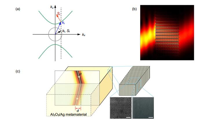 Figure 3. (a) Hyperbolic dispersion relationship in nanowire array structure [17]. (b) Simulated negative refraction of hyperbolic metamaterials [16]. (c) Schematic of a silver nanowire hyperbolic metamaterial as well as scanning electron microscopy images showing the top and side views of the nanowires. The scale bars indicate 500 nm [18].
2.3.2 超分辨成像
双曲超材料不仅可以实现光学负折射效应,还可以用来实现亚波长超分辨成像。众所周知,利用传统光学透镜成像,通常会受光学衍射极限的限制,其中丢失的超越衍射极限的图像信息由倏逝波携带。倏逝波由于具有大的面内波矢,在空气及光学透镜中都不能传播。然而,正如之前2.1节中提到的,双曲超材料由于其独特的色散特性能够支持任意波矢的波向前传播。因此Jacob等人选择用双曲超材料来传输成像物体的倏逝波[6, 45-46],基于这种设计原理的透镜称为双曲超透镜。
如图 4(a)所示,由平板形金属介质多层膜结构演化而来的圆柱形双曲超透镜可以实现超越衍射极限的放大成像。在圆柱超透镜内部,物点散射的电磁波在内部物面被接收,经由弯曲超透镜传播,在成像面得到放大的像。这时物体所成的像已经在衍射极限范围内,从而达到超越衍射极限的远场成像效果。图 4(b)画出了沿切向层叠和径向层叠设计超透镜的两种思路。目前已经在多个波段实验实现了双曲超透镜的亚波长成像[7, 9]。如图 4(c)所示,Liu等人在石英半圆柱衬底上镀上16层Ag和Al2O3薄膜[7],利用金属介质膜的双曲色散特性和波矢缩放特性,成功将宽度35 nm、间隔150 nm的两根纳米线图样分开。在365 nm波长入射时,这种超透镜的最高分辨率能够达到130 nm。
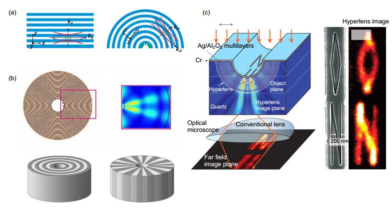 Figure 4. (a) Schematic of the planar and cylindrical multilayer hyperbolic structures and their dispersion properties [47]. (b) Schematic of hyperlens and its simulation results (up) and possible realizations of hyperlens——concentric metallic layers alternate with dielectric layers or radially symmetric "slices" alternate in composition between metallic and dielectric (down) [6]. (c) Left: Schematic of the hyperlens and the incident wavelength is 365 nm, Right: The beyond-diffraction image of the word "ON" [7].
理论计算显示,这种双曲超透镜的分辨率由有效波长决定:
\Delta \propto \frac{{{R_{{\rm{inner}}}}}}{{{R_{{\rm{outer}}}}}}\lambda, (8) 其中:Rinner和Router分别为双曲超透镜的内径和外径,λ为工作波长。
3. 双曲超表面
在操控电磁波方面,尽管三维双曲超材料凭借其特有的色散特性超越传统方法,但它们存在结构加工复杂以及在高频段损耗较大的缺陷,从而限制了其应用范围。双曲超表面(hyperbolic metasurfaces,HMTSs)可以看成是二维平面的双曲超材料,它不仅具有三维双曲超材料所特有的性质,同时还能够有效克服三维双曲超材料的缺陷,如能实现大面积加工,降低体材料损耗和与其他光电器件兼容等。
另外,关于超表面的研究主要集中于对电磁波的远场调控[48-53],而双曲超表面的特殊性质得益于表面等离子激元的激发[54-56],因此通过调节结构表面的等离子激元,可以实现对面内和近场电磁波的调控。这一特点使双曲超表面在超表面研究中独树一帜。
3.1 双曲超表面的色散机制
双曲超表面作为二维平面上的单轴材料,其介电常数同样也是张量形式。因为制作这种超表面的材料多为二维材料,如石墨烯、二硫化钼等,因此计算时更习惯于用电导率张量来替代介电常数张量:
\mathit{\boldsymbol{\sigma }} = \left[{\begin{array}{*{20}{c}} {{\sigma _{xx}}}&0\\ 0&{{\sigma _{yy}}} \end{array}} \right], (9) Gomez-Diaz等人计算出表面单轴材料中横磁波的色散关系[57]
\begin{array}{c} \eta _0^2{(k_x^2{\sigma _{xx}} + k_y^2{\sigma _{yy}})^2}(k_x^2 + k_y^2-k_0^2)-\\ 4k_0^2{(k_x^2 + k_y^2)^2} = 0, \end{array} (10) 当电导率分量的虚部均大于零时,材料表面为电感表面,能够传导表面等离子激元,同时色散拓扑结构为圆或椭圆,如图 5(a)中,曲线的电导率为 {\sigma _{xx}} = {\sigma _{yy}} = 0.05 + {\rm{i}}23.5\;{\rm{ \mathsf{ μ} S}} 。若电导率分量不相等,表面能量会向虚部较小的分量方向集中,均一的单层石墨烯就是这种拓扑结构一个典型的例子。当电导率分量的虚部符号不同时,材料呈现双曲拓扑结构,如图 5(b)所示,这种拓扑结构的渐近线方程可近似表示为

{k_y} = \pm m{k_x} \pm b, (11) 其中:
m = \sqrt {-\frac{{{\sigma _{xx}}}}{{{\sigma _{yy}}}}}, b = {k_0}\sqrt {1 + {{\left( {\frac{2}{{{\eta _0}{\sigma _{yy}}}}} \right)}^2}} 。 在理想情况下,这种拓扑结构材料能够无限地将电磁波束缚在面内的某些方向[58],束缚张角为 \phi = \arctan [\pm \sqrt {-({\sigma _{xx}}/{\sigma _{yy}})}] 。另外,值得一提的是,在椭圆和双曲的转变点,拓扑结构会被无限压缩,色散曲线几近平坦,如图 5(c)所示。在这种情况下,电导率张量某一分量虚部远大于另一分量,材料能够传输表面等离子激元而几乎不发生衍射现象,即所谓的无衍射传输[5]。在电导率分量符号相反的前提下,图 5(c)的色散曲线可以看成图 5(b)的极端情况。图 5(a)~5(c)均讨论的是材料无损耗或损耗较小的情况,此时双曲色散曲线敞开。当材料的损耗较大时,电导率实部的绝对值与虚部的绝对值相当,这时双曲色散由敞开转为闭合,图 5(d)中电导率分量为 {\sigma _{xx}} = 0.08 + {\rm{i0}}{\rm{.1}}\;{\rm{mS}} , {\sigma _{yy}} = 0.08-{\rm{i0}}{\rm{.1}}\;{\rm{mS}} ,实部与虚部相差很小,此时色散曲线会出现最大的截止波矢。
3.2 双曲超表面的实现方法
为了实现双曲超表面的色散关系,Gomez-Diaz等人提出了三种可以尝试的策略[12]。首先可以从自然界存在的三维双曲晶体材料入手,比如常见的石墨,由多层平行排列的石墨烯组合,并且层与层之间通过范德瓦耳斯力结合。沿每层平面方向表现为金属性,即介电常数实部为负,而与层面垂直方向,其介电常数为正,这正好满足了双曲色散所需条件。因此,在紫外波段,石墨为天然存在的双曲材料[35]。除此以外,在可见光波段有类似特性的材料有二硼化镁MgB2晶体[59-60],以及红外波段的高温超导体钇钡铜氧[61-62]、镧锶铜氧[63]还有六方氮化硼h-BN[64-65]、金属铋[66]等,都属于天然双曲材料。当将这些晶体材料减薄至亚波长量级时就形成具有双曲色散特性的表面结构。
另一种方法是直接寻找天然存在的二维双曲材料,这样避免了减薄过程的复杂工艺以及减薄可能带来的尺寸效应。最近研究较多的二维材料中[67],黑磷具有极端各向异性[68-72],是天然的二维双曲材料。
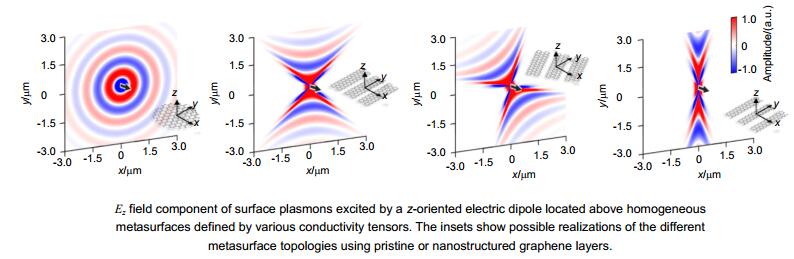
除了以上两种方法之外,还可以通过用亚波长尺度上电磁有序结构来实现人工双曲超表面的构建。人工双曲超表面不仅能够摆脱天然材料本身内部晶体结构的限制,而且为电磁场调控提供了前所未有的灵活性。石墨烯本身表面各向同性且具有电磁可调性,是制备双曲超表面的首选材料。图 6(a)是一组利用石墨烯条带阵列实现的超表面结构设计[57],它是将石墨烯裁剪成特定宽度的条带状,再按一定周期平行排布,组合成条带阵列。条带阵列的周期远远小于石墨烯表面等离子体的波长。这样,石墨烯表面沿条带方向与垂直条带方向的电导率不再相同。可以看到,这种设计能够从各向同性圆色散拓扑转变为其它色散结构。图 6(b)为这种条带结构沿y(上图)和x(下图)方向的电导率虚部随条带宽度W及频率的变化关系谱图。可见y方向电导率虚部Im(σyy)的值一直为正,而Im(σxx)却随着W的变化存在一个突变点。在突变点左侧符号为负,色散呈双曲线型;在突变点右侧符号为正,色散呈圆或椭圆。因此,通过调节石墨烯条带宽度就能够改变超表面的拓扑结构。另外,通过调节石墨烯化学势,还可以操控双曲拓扑结构的主轴方向及张角大小。其他的关于利用石墨烯制作双曲超表面的研究表明,双曲效应不仅可以用电场控制,同时也可以用磁场来实现[73]。除此之外,在3.3.2节中我们还会详细举例说明如何将已有的块体双曲超材料压缩到二维平面,以实现双曲超表面的设计。
 Figure 6. (a) Ez field component of surface plasmons excited by a z-oriented electric dipole located above homogeneous metasurfaces defined by various conductivity tensors. The insets show possible realizations of the different metasurface topologies using pristine or nanostructured graphene layers [57]. (b) The imaginary part of the effective electric conductivity along y (up) and x (down) direction versus ribbon width W [57].
3.3 双曲超表面几种典型的应用
双曲超表面与双曲超材料极其相似的色散特性决定了它们相似的应用研究方向。而二维双曲超表面拥有损耗小、集成度强、能大面积加工等优于三维块体双曲超材料的特点。本节主要介绍双曲超表面在负折射效应、超透镜成像、局域场增强效应等方面的应用。
3.3.1 负折射效应
与三维块体双曲超材料类似,双曲超表面也具有负折射效应。Liu等人早在2013年就理论设计出由周期性Ag光栅构成的超表面[74],如图 7(a)所示。当入射光波长为633 nm时,其结构表面等离子激元色散分布呈上凸线型(图 7(b));当入射光波长变为500 nm时,其色散分布又变成双曲线型,具有负折射效应(图 7(c));当波长为543 nm时,超表面则呈现两种线型的过渡态,即近平坦线型,说明它位于拓扑结构的转变点附近。具有不同色散关系的表面等离子激元波会产生不同的传播现象,如图 7(d)~7(f)所示,入射光波长为500 nm,部分光源由于负折射在光栅外部重新聚焦,类似Veselago透镜[1]。入射光波长为543 nm时,形成几乎无衍射的表面等离子激元传输,也就是说由超表面一端光源发出的所有电磁波包括倏逝波,会被完整地传播到超表面的另一端。这一现象也是前面提到的超透镜成像的基础。图 8为相应的实验结果,单晶Ag光栅超表面在不同波长光以特定角度入射时的折射响应[75]。
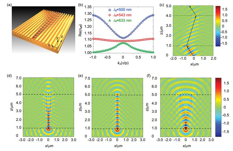 Figure 7. (a) Schematic of metasurface based on grating structure [74]. (b) The dispersion relationship of the grating metasurface at different wavelengths. The grating period is 120 nm, the width is 60 nm and the height is 80 nm [74]. (c) The simulated negative refraction of the grating metasurface with 500 nm incident wave. The grating period is 100 nm, the width is 40 nm and the height is 100 nm [74]. (d)~(f) Propagation of surface plasmons along the metasurface at three different wavelengths of (d) 500 nm, (e) 543 nm and (f) 633 nm [74].
3.3.2 超透镜成像
前面提到利用拓扑结构转变点附近的近平坦色散特性可以实现结构表面等离子体模式无衍射传输,这为超透镜的实现奠定了基础[73, 76-78]。Alexander等人在研究Ag光栅超表面的负折射效应的同时,也成功观察到了结构中的无衍射传输现象[75]。
除了金属材料,二维材料石墨烯也是制备超透镜的热门之选。图 9(a)为Gomez-Diaz等人模拟的单层石墨烯超透镜示意图[12]。黑色实线左测边的区域为各向同性,右测区域为双曲超表面,并且处于拓扑转变结构点附近,它的等频线中ky几乎不随kx而改变,因此能保持直线传输。在界面上方放置两个电偶极子源,频率10 THz,电偶极子的间距大约为真空中波长的0.007倍,同时在距界面两侧等距离处观测。观测的电场z分量结果如图 9(b)所示。发现尽管间距远远小于真空中波长,但双曲超表面仍然能恢复光源的像并将亚波长细节完美保留。
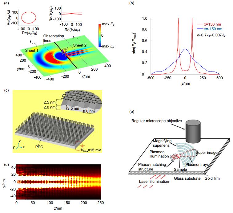 Figure 9. (a) Schematic of the non-diffraction transmission of the monolayer graphene [12]. (b) The normalized z component of the electric field at the observation lines in Figure (a) [12]. (c) The method of adding substrate and bias to transform graphene to hyperbolic metasurface [5]. (d) Simulated SPPs propagation on the graphene metasurface in Figure (c) [5]. (e) Schematic of the planar magnifying hyperlens [79].
Forati等人进一步提出将各向同性石墨烯转化为双曲超表面的方法[5]。他们的设计思路如下:将单层石墨烯紧贴在周期起伏的基底上,然后在结构的上下表面加一定的电压,石墨烯会由于基底的作用在两个方向上产生不同的电导率,从而由各向同性表面变为各向异性表面,甚至变为处于拓扑转变点附近的双曲超表面,结构示意图如图 9(c)。通过参数优化,这种结构能够在太赫兹波段实现无衍射传输,并且能够容许真实损耗的存在,图 9(d)显示了仿真结果。
双曲超表面从双曲超材料演化而来,在设计思路上可以相互借鉴。基于块体超透镜的设计,Smolyaninov等人也在平面上提出了类似的超透镜成像[79],如图 9(e)所示。在该结构的设计中,能够利用传统镜头来探测物体的远场超分辨成像。
3.3.3 局域场增强
由于双曲超表面支持的等离子激元传播波矢没有上限,它能与周围任意取向的散射体相互作用,如图 10(a)所示[80],从而增强它们的自发辐射率。与块体双曲超材料相比,双曲超表面在与表面垂直的方向具有倏逝场,能有效增强电磁场在表面的局域和强度[58]。
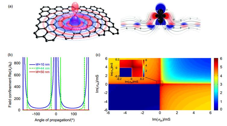
前面提到在石墨烯带状阵列结构中,可以通过调节结构参数和负载电压实现色散曲线的自由调控。当色散曲线为双曲线时,在特定角度它能产生非常强的场局域作用,如图 10(b)所示。需要注意的是,由于在实际操作中损耗的存在,使无限延伸的色散曲线闭合,场的局域效应会被不可避免地削弱。
类比块体双曲超材料的局域场增强效应[24, 29, 81],一个放置在超表面附近的任意取向辐射体的自发辐射率(SER,用RSE表示),或Purcell因子可以用以下公式来描述[82]:
\begin{array}{l} {R_{{\rm{SE}}}} = \frac{P}{{{P_0}}} = \\ \;\;\;\;\;\;\;\;\;1 + \frac{{6{\rm{ \mathit{ π} }}}}{{|{\mathit{\boldsymbol{\mu }}_\rho }|{k_0}}}{\mathit{\boldsymbol{\mu }}_\rho } \cdot {\mathop{\rm Im}\nolimits} [{\mathit{\boldsymbol{G}}_{\rm{s}}}({\mathit{\boldsymbol{r}}_0}, {\mathit{\boldsymbol{r}}_0}, \omega )] \cdot {\mathit{\boldsymbol{\mu }}_\rho }, \end{array} (12) 其中: {\mathit{\boldsymbol{G}}_{\rm{s}}}({\mathit{\boldsymbol{r}}_0}, {\mathit{\boldsymbol{r}}_0}, \omega ) 为超表面存在时的格林函数的散射分量, {\mathit{\boldsymbol{\mu }}_\rho } 为沿着辐射方向的单位矢量,k0为自由空间波数,r0为源的位置,P,P0分别为电偶极子在非均质环境和自由空间中的辐射能量。图 10(c)为利用式(12)计算出的自发辐射率与超表面电导率张量的对应关系。其中二四象限对应着双曲色散,一三象限分别对应椭圆色散和横电波模式,二四象限的自发辐射率SER值明显高于一三象限,说明双曲色散确实有增强自发辐射的效果。另外,电导率张量越接近拓扑转变点(图 10(c)中用虚线框标记部分),超表面的自发辐射率SER越高。可以理解为,在接近拓扑转变点时,色散曲线变得更平坦,更大波矢的波也能够耦合进超表面,场增强也更大。
3.3.4 其他
局域场增强效应除了可以用来提高自发辐射率外,还可以被用来增强热辐射。理论和实验研究表明,在能支持表面等离子激元传播或者满足双曲色散的条件下,近场热流辐射能够超越远场热辐射Stefan- Boltzmann定律的限制,并且能高出多个数量级[83-85]。Liu等人设计了一种利用石墨烯带状阵列增强近场热辐射的结构[86]。此外,双曲超材料还可用来设计电磁吸收器[87],或用于探索等离子体的自旋霍尔效应[75, 88]。
4. 局限与展望
双曲超表面的应用主要基于其具有极大波矢的特性,然而在实际应用中具有较大波矢的倏逝波与超表面的耦合却非常弱[89-90]。这主要有以下三个方面的原因:第一、材料损耗。当材料存在损耗时,原本无限延伸的双曲色散曲线会闭合,导致无法支持长波矢的传输;第二、与人工结构周期性有关的非局域性,导致在布洛赫边界出现截止波数,周期性的影响大于材料损耗的影响。第三、双曲超表面构成材料的本征非局域性[91-92],也会造成双曲线闭合,且非局域性的影响大于前两者。所幸的是非局域性影响可以通过调节结构参数来避免。
双曲超表面不仅仅在纵向维度尺寸上实现了大幅度减少,同时还伴随着很多新奇的应用前景,譬如与柔性基底集成,与电路或者生物器件相容,或者制成可穿戴式设备,同时它的负折射效应也可以用来做隐形斗篷,无衍射传输除了用来做超透镜外,还可以做光耦合器等。
-

图 2 (a) 金属-介质多层膜结构示意图,ε、μ、d分别代表材料的介电常数、磁导率和薄膜厚度[20]. (b)半导体多层膜结构有效介电常数的实部图,ε⊥、ε||分别表示垂直和平行于多层膜的介电常数[15]. (c)金属纳米线阵列结构示意图,d为金属纳米线阵列周期,r为金属纳米线半径[16].
Figure 2. (a) Schematic of the metal-dielectric multilayer structure, ε, μ, d represent the permittivity, permeability and film thickness respectively [20]. (b) The real part of the permittivity of a semiconductor multilayer structure, ε⊥, ε|| represent the permittivity that are perpendicular and parallel to the film, respectively [15]. (c) Schematic diagram of the nanowire array structure, d is the period of the nanowire array and r is the radius of the metal nanowire [16].
图 3 (a) 基于金属纳米线阵列的双曲超材料的色散特性[17]. (b)理论计算的双曲超材料的负折射现象[16]. (c)利用氧化铝模板制备的金属银纳米线阵列,SEM照片中标尺为500 nm [18].
Figure 3. (a) Hyperbolic dispersion relationship in nanowire array structure [17]. (b) Simulated negative refraction of hyperbolic metamaterials [16]. (c) Schematic of a silver nanowire hyperbolic metamaterial as well as scanning electron microscopy images showing the top and side views of the nanowires. The scale bars indicate 500 nm [18].
图 4 (a) 基于金属介质多层膜的平板形和圆柱形双曲超材料及其各自色散曲线[47]. (b)上图:双曲超透镜结构示意图及仿真结果.下图:双曲超透镜的两种设计思路,切向层叠和径向层叠[6]. (c)左图:超透镜结构示意图,入射波长365 nm;右图:字母“ON”的超越衍射极限图样[7].
Figure 4. (a) Schematic of the planar and cylindrical multilayer hyperbolic structures and their dispersion properties [47]. (b) Schematic of hyperlens and its simulation results (up) and possible realizations of hyperlens——concentric metallic layers alternate with dielectric layers or radially symmetric "slices" alternate in composition between metallic and dielectric (down) [6]. (c) Left: Schematic of the hyperlens and the incident wavelength is 365 nm, Right: The beyond-diffraction image of the word "ON" [7].
图 5 (a) ~(c)当z取向的电偶极子(黑色箭头)位于表面上方时,在不同电导率情况下表面电场z分量的响应,插图为色散等频曲线[12]. (d)损耗较大时的表面等离子激元传播及其等频曲线[58].
Figure 5. (a)~(c) Color maps show the z-component of the electric field excited by a z-directed dipole (black arrow) located above the surface. The insets present the isofrequency contour of each metasurface topology[12]. (d) In the case that the loss cannot be ignored [58].
图 6 (a) 石墨烯超表面上传播的表面等离子体的电场z分量,插图为对应的石墨烯超表面结构示意图[57]. (b)石墨烯超表面x, y垂直方向的电导率虚部随条带宽度和频率变化的谱图,上图对应y方向,下图对应x方向[57].
Figure 6. (a) Ez field component of surface plasmons excited by a z-oriented electric dipole located above homogeneous metasurfaces defined by various conductivity tensors. The insets show possible realizations of the different metasurface topologies using pristine or nanostructured graphene layers [57]. (b) The imaginary part of the effective electric conductivity along y (up) and x (down) direction versus ribbon width W [57].
图 7 (a) 基于光栅结构的超表面结构示意图[74]. (b)光栅在不同入射光下的色散分布图,光栅周期120 nm,宽度60 nm,高度80 nm[74]. (c)光栅超表面的负折射效应,入射波长500 nm,光栅周期100 nm,宽度40 nm,高度100 nm[74]. (d)~(f)入射波长分别为500 nm(左),543 nm(中),633 nm(右)时结构表面等离子激元波传播[74].
Figure 7. (a) Schematic of metasurface based on grating structure [74]. (b) The dispersion relationship of the grating metasurface at different wavelengths. The grating period is 120 nm, the width is 60 nm and the height is 80 nm [74]. (c) The simulated negative refraction of the grating metasurface with 500 nm incident wave. The grating period is 100 nm, the width is 40 nm and the height is 100 nm [74]. (d)~(f) Propagation of surface plasmons along the metasurface at three different wavelengths of (d) 500 nm, (e) 543 nm and (f) 633 nm [74].

图 9 (a) 单层石墨烯无衍射传输示意图[12]. (b)图(a)虚线观察线处的电场强度z分量归一化结果[12]. (c)石墨烯加衬底,加偏压转化为双曲超表面的方法示意图[5]. (d)两个电偶极子经过图(c)中石墨烯表面的仿真结果[5]. (e)平面放大超透镜结构示意图[79].
Figure 9. (a) Schematic of the non-diffraction transmission of the monolayer graphene [12]. (b) The normalized z component of the electric field at the observation lines in Figure (a) [12]. (c) The method of adding substrate and bias to transform graphene to hyperbolic metasurface [5]. (d) Simulated SPPs propagation on the graphene metasurface in Figure (c) [5]. (e) Schematic of the planar magnifying hyperlens [79].
图 10 (a) 石墨烯表面散射体辐射电磁波与表面等离子激元耦合示意图[80]. (b)不同传播角度下的场局域性[58]. (c)自发辐射率随电导率虚部的变化[58].
Figure 10. (a) Schematic of the coupling of a dipole emitter to graphene SPPs [80]. (b) Field confinement at different angles of propagation [58]. (c) SER in logarithm scale versus the conductivity components of the structure [58].
-
参考文献
[1] Pendry J B. Negative refraction makes a perfect lens[J]. Physical Review Letters, 2000, 85(18): 3966-3969. doi: 10.1103/PhysRevLett.85.3966
[2] Shelby R A, Smith D R, Schultz S. Experimental verification of a negative index of refraction[J]. Science, 2001, 292(5514): 77-79. doi: 10.1126/science.1058847
[3] Naik G V, Saha B, Liu Jing, et al. Epitaxial superlattices with titanium nitride as a plasmonic component for optical hyperbolic metamaterials[J]. Proceedings of the National Academy of Sciences of the United States of America, 2014, 111(21): 7546-7551. doi: 10.1073/pnas.1319446111
[4] Esfandyarpour M, Garnett E C, Cui Yi, et al. Metamaterial mirrors in optoelectronic devices[J]. Nature Nanotechnology, 2014, 9(7): 542-547. doi: 10.1038/nnano.2014.117
[5] Forati E, Hanson G W, Yakovlev A B, et al. Planar hyperlens based on a modulated graphene monolayer[J]. Physical Review B, 2014, 89(8): 081410. doi: 10.1103/PhysRevB.89.081410
[6] Jacob Z, Alekseyev L V, Narimanov E. Optical hyperlens: far-field imaging beyond the diffraction limit[J]. Optics Express, 2006, 14(18): 8247-8256. doi: 10.1364/OE.14.008247
[7] Liu Zhaowei, Lee H, Xiong Yi, et al. Far-field optical hyperlens magnifying sub-diffraction-limited objects[J]. Science, 2007, 315(5819): 1686. doi: 10.1126/science.1137368
[8] Narimanov E E, Shalaev V M. Optics: beyond diffraction[J]. Nature, 2007, 447(7142): 266-267. doi: 10.1038/447266a
[9] Rho J, Ye Ziliang, Xiong Yi, et al. Spherical hyperlens for two-dimensional sub-diffractional imaging at visible frequencies[J]. Nature Communications, 2010, 1: 143. doi: 10.1038/ncomms1148
[10] Yao Jie, Yang Xiaodong, Yin Xiaobo, et al. Three-dimensional nanometer-scale optical cavities of indefinite medium[J]. Proceedings of the National Academy of Sciences of the United States of America, 2011, 108(28): 11327-11331. doi: 10.1073/pnas.1104418108
[11] Jacob Z, Smolyaninov I I, Narimanov E E. Broadband Purcell effect: radiative decay engineering with metamaterials[J]. Applied Physics Letters, 2012, 100(18): 181105. doi: 10.1063/1.4710548
[12] Gomez-Diaz J S, Alù A. Flatland optics with hyperbolic metasurfaces[J]. ACS Photonics, 2016, 3(12): 2211-2224. doi: 10.1021/acsphotonics.6b00645
[13] Poddubny A, Iorsh I, Belov P, et al. Hyperbolic metamaterials[J]. Nature Photonics, 2013, 7(12): 948-957. doi: 10.1038/nphoton.2013.243
[14] Lu D, Kan J J, Fullerton E E, et al. Enhancing spontaneous emission rates of molecules using nanopatterned multilayer hyperbolic metamaterials[J]. Nature Nanotechnology, 2014, 9(1): 48-53. doi: 10.1038/nnano.2013.276
[15] Hoffman A J, Alekseyev L, Howard S S, et al. Negative refraction in semiconductor metamaterials[J]. Nature Materials, 2007, 6(12): 946-950. doi: 10.1038/nmat2033
[16] Liu Yongmin, Bartal G, Zhang Xiang. All-angle negative refraction and imaging in a bulk medium made of metallic nanowires in the visible region[J]. Optics Express, 2008, 16(20): 15439-15448. doi: 10.1364/OE.16.015439
[17] Yao Jie, Wang Yuan, Tsai K T, et al. Design, fabrication and characterization of indefinite metamaterials of nanowires[J]. Philosophical Transactions of the Royal Society A: Mathematical, Physical and Engineering Sciences, 2011, 369(1950): 3434-3446. doi: 10.1098/rsta.2011.0159
[18] Yao Jie, Liu Zhaowei, Liu Yongmin, et al. Optical negative refraction in bulk metamaterials of nanowires[J]. Science, 2008, 321(5891): 930. doi: 10.1126/science.1157566
[19] Choy T C. Effective Medium Theory: Principles and Applications[M]. 2nd ed. New York: Oxford University Press, 2015.
[20] Wood B, Pendry J B, Tsai D P. Directed subwavelength imaging using a layered metal-dielectric system[J]. Physical Review B, 2006, 74(11): 115116. doi: 10.1103/PhysRevB.74.115116
[21] Ferrari L, Wu C, Lepage D, et al. Hyperbolic metamaterials and their applications[J]. Progress in Quantum Electronics, 2015, 40: 1-40. doi: 10.1016/j.pquantelec.2014.10.001
[22] Jacob Z, Kim J Y, Naik G V, et al. Engineering photonic density of states using metamaterials[J]. Applied Physics B, 2010, 100(1): 215-218. doi: 10.1007/s00340-010-4096-5
[23] Kim J, Drachev V P, Jacob Z, et al. Improving the radiative decay rate for dye molecules with hyperbolic metamaterials[J]. Optics Express, 2012, 20(7): 8100-8116. doi: 10.1364/OE.20.008100
[24] Shalaginov M Y, Ishii S, Liu J, et al. Broadband enhancement of spontaneous emission from nitrogen-vacancy centers in nanodiamonds by hyperbolic metamaterials[J]. Applied Physics Letters, 2013, 102(17): 173114. doi: 10.1063/1.4804262
[25] Ni X, Naik G V, Kildishev A V, et al. Effect of metallic and hyperbolic metamaterial surfaces on electric and magnetic dipole emission transitions[J]. Applied Physics B, 2011, 103(3): 553-558. doi: 10.1007/s00340-011-4468-5
[26] Sreekanth K V, Biaglow T, Strangi G. Directional spontaneous emission enhancement in hyperbolic metamaterials[J]. Journal of Applied Physics, 2013, 114(13): 134306. doi: 10.1063/1.4824287
[27] Tumkur T, Zhu G, Black P, et al. Control of spontaneous emission in a volume of functionalized hyperbolic metamaterial[J]. Applied Physics Letters, 2011, 99(15): 151115. doi: 10.1063/1.3631723
[28] Tumkur T U, Gu Lei, Kitur J K, et al. Control of absorption with hyperbolic metamaterials[J]. Applied Physics Letters, 2012, 100(16): 161103. doi: 10.1063/1.4703931
[29] Krishnamoorthy H N S, Jacob Z, Narimanov E, et al. Topological transitions in metamaterials[J]. Science, 2012, 336(6078): 205-209. doi: 10.1126/science.1219171
[30] Naik G V, Liu Jingjing, Kildishev A V, et al. Demonstration of Al: ZnO as a plasmonic component for near-infrared metamaterials[J]. Proceedings of the National Academy of Sciences of the United States of America, 2012, 109(23): 8834-8838. doi: 10.1073/pnas.1121517109
[31] Yang Xiaodong, Yao Jie, Rho J, et al. Experimental realization of three-dimensional indefinite cavities at the nanoscale with anomalous scaling laws[J]. Nature Photonics, 2012, 6(7): 450-454. doi: 10.1038/nphoton.2012.124
[32] Evans P, Hendren W R, Atkinson R, et al. Growth and properties of gold and nickel nanorods in thin film alumina[J]. Nanotechnology, 2006, 17(23): 5746-5753. doi: 10.1088/0957-4484/17/23/006
[33] Noginov M A, Li H, Barnakov Y A, et al. Controlling spontaneous emission with metamaterials[J]. Optics Letters, 2010, 35(11): 1863-1865. doi: 10.1364/OL.35.001863
[34] Nefedov I S. Electromagnetic waves propagating in a periodic array of parallel metallic carbon nanotubes[J]. Physical Review B, 2010, 82(15): 155423. doi: 10.1103/PhysRevB.82.155423
[35] Sun Jingbo, Zhou Ji, Li Bo, et al. Indefinite permittivity and negative refraction in natural material: graphite[J]. Applied Physics Letters, 2011, 98(10): 101901. doi: 10.1063/1.3562033
[36] Wurtz G A, Pollard R, Hendren W, et al. Designed ultrafast optical nonlinearity in a plasmonic nanorod metamaterial enhanced by nonlocality[J]. Nature Nanotechnology, 2011, 6(2): 107-111. doi: 10.1038/nnano.2010.278
[37] Kabashin A V, Evans P, Pastkovsky S, et al. Plasmonic nanorod metamaterials for biosensing[J]. Nature Materials, 2009, 8(11): 867-871. doi: 10.1038/nmat2546
[38] Parazzoli C G, Greegor R B, Li K, et al. Experimental verification and simulation of negative index of refraction using Snell's law[J]. Physical Review Letters, 2003, 90(10): 107401. doi: 10.1103/PhysRevLett.90.107401
[39] Smith D R, Schurig D. Electromagnetic wave propagation in media with indefinite permittivity and permeability tensors[J]. Physical Review Letters, 2003, 90(7): 077405. doi: 10.1103/PhysRevLett.90.077405
[40] Cubukcu E, Aydin K, Ozbay E, et al. Electromagnetic waves: negative refraction by photonic crystals[J]. Nature, 2003, 423(6940): 604-605. https://www.researchgate.net/publication/260626030_Electromagnetic_waves_Negative_refraction_by_photonic_crystals
[41] Parimi P V, Lu Wentao, Vodo P, et al. Photonic crystals: imaging by flat lens using negative refraction[J]. Nature, 2003, 426(6965): 404. doi: 10.1038/426404a
[42] Berrier A, Mulot M, Swillo M, et al. Negative refraction at infrared wavelengths in a two-dimensional photonic crystal[J]. Physical Review Letters, 2004, 93(7): 073902. doi: 10.1103/PhysRevLett.93.073902
[43] Schonbrun E, Wu Qi, Park W, et al. Wave front evolution of negatively refracted waves in a photonic crystal[J]. Applied Physics Letters, 2007, 90(4): 041113. doi: 10.1063/1.2435344
[44] Wangberg R, Elser J, Narimanov E E, et al. Nonmagnetic nanocomposites for optical and infrared negative-refractive- index media[J]. Journal of the Optical Society of America B, 2006, 23(3): 498-505. doi: 10.1364/JOSAB.23.000498
[45] Salandrino A, Engheta N. Far-field subdiffraction optical microscopy using metamaterial crystals: theory and simulations[J]. Physical Review B, 2006, 74(7): 075103. doi: 10.1103/PhysRevB.74.075103
[46] Silveirinha M G, Belov P A, Simovski C R. Subwavelength imaging at infrared frequencies using an array of metallic nanorods[J]. Physical Review B, 2007, 75(3): 035108. doi: 10.1103/PhysRevB.75.035108
[47] Lu D, Liu Zhaowei. Hyperlenses and metalenses for far-field super-resolution imaging[J]. Nature Communications, 2012, 3: 1205. doi: 10.1038/ncomms2176
[48] Lin Dianmin, Fan Pengyu, Hasman E, et al. Dielectric gradient metasurface optical elements[J]. Science, 2014, 345(6194): 298-302. doi: 10.1126/science.1253213
[49] Arbabi A, Horie Y, Bagheri M, et al. Dielectric metasurfaces for complete control of phase and polarization with subwavelength spatial resolution and high transmission[J]. Nature Nanotechnology, 2015, 10(11): 937-943. doi: 10.1038/nnano.2015.186
[50] Yu Nanfang, Capasso F. Flat optics with designer metasurfaces[J]. Nature Materials, 2014, 13(2): 139-150. doi: 10.1038/nmat3839
[51] Yu Nanfang, Genevet P, Kats M A, et al. Light propagation with phase discontinuities: generalized laws of reflection and refraction[J]. Science, 2011, 334(6054): 333-337. doi: 10.1126/science.1210713
[52] Khorasaninejad M, Chen Weiting, Devlin R C, et al. Metalenses at visible wavelengths: diffraction-limited focusing and subwavelength resolution imaging[J]. Science, 2016, 352(6290): 1190-1194. doi: 10.1126/science.aaf6644
[53] Kildishev A V, Boltasseva A, Shalaev V M. Planar photonics with metasurfaces[J]. Science, 2013, 339(6125): 1232009. doi: 10.1126/science.1232009
[54] Sun Shulin, He Qiong, Xiao Shiyi, et al. Gradient-index meta-surfaces as a bridge linking propagating waves and surface waves[J]. Nature Materials, 2012, 11(5): 426-431. doi: 10.1038/nmat3292
[55] Genevet P, Lin Jiao, Kats M A, et al. Holographic detection of the orbital angular momentum of light with plasmonic photodiodes[J]. Nature Communications, 2012, 3: 1278. doi: 10.1038/ncomms2293
[56] Lin Jiao, Mueller J P B, Wang Qian, et al. Polarization-controlled tunable directional coupling of surface Plasmon polaritons[J]. Science, 2013, 340(6130): 331-334. doi: 10.1126/science.1233746
[57] Gomez-Diaz J S, Tymchenko M, Alù A. Hyperbolic metasurfaces: surface plasmons, light-matter interactions, and physical implementation using graphene strips[Invited][J]. Optical Materials Express, 2015, 5(10): 2313-2329. doi: 10.1364/OME.5.002313
[58] Gomez-Diaz J S, Tymchenko M, Alù A. Hyperbolic plasmons and topological transitions over uniaxial metasurfaces[J]. Physical Review Letters, 2015, 114(23): 233901. doi: 10.1103/PhysRevLett.114.233901
[59] Belashchenko K D, van Schilfgaarde M, Antropov V P. Coexistence of covalent and metallic bonding in the boron intercalation superconductor MgB2[J]. Physical Review B, 2001, 64(9): 092503. doi: 10.1103/PhysRevB.64.092503
[60] Guritanu V, Kuzmenko A B, van der Marel D, et al. Anisotropic optical conductivity and two colors of MgB2[J]. Physical Review B, 2006, 73(10): 104509. doi: 10.1103/PhysRevB.73.104509
[61] Nee T W. Anisotropic optical properties of YBa2Cu3O7[J]. Journal of Applied Physics, 1992, 71(12): 6002-6007. doi: 10.1063/1.350454
[62] Korzeb K, Gajc M, Pawlak D A. Compendium of natural hyperbolic materials[J]. Optics Express, 2015, 23(20): 25406- 25424. doi: 10.1364/OE.23.025406
[63] Sun Jingbo, Litchinitser N M, Zhou Ji. Indefinite by nature: from ultraviolet to terahertz[J]. ACS Photonics, 2014, 1(4): 293-303. doi: 10.1021/ph4000983
[64] Caldwell J D, Kretinin A V, Chen Yiguo, et al. Sub-diffractional volume-confined polaritons in the natural hyperbolic material hexagonal boron nitride[J]. Nature Communications, 2014, 5: 5221. doi: 10.1038/ncomms6221
[65] Dai S, Fei Z, Ma Q, et al. Tunable phonon polaritons in atomically thin van der Waals crystals of boron nitride[J]. Science, 2014, 343(6175): 1125-1129. doi: 10.1126/science.1246833
[66] Alekseyev L V, Podolskiy V A, Narimanov E E. Homogeneous hyperbolic systems for terahertz and far-infrared frequencies[J]. Advances in Optoelectronics, 2012, 2012: 267564. https://www.researchgate.net/publication/258383047_Homogeneous_Hyperbolic_Systems_for_Terahertz_and_Far-Infrared_Frequencies
[67] Gupta A, Sakthivel T, Seal S. Recent development in 2D materials beyond graphene[J]. Progress in Materials Science, 2015, 73: 44-126. doi: 10.1016/j.pmatsci.2015.02.002
[68] Low T, Roldán R, Wang Han, et al. Plasmons and screening in monolayer and multilayer black phosphorus[J]. Physical Review Letters, 2014, 113(10): 106802. doi: 10.1103/PhysRevLett.113.106802
[69] Rodin A S, Carvalho A, Castro Neto A H. Strain-induced gap modification in black phosphorus[J]. Physical Review Letters, 2014, 112(17): 176801. doi: 10.1103/PhysRevLett.112.176801
[70] Low T, Rodin A S, Carvalho A, et al. Tunable optical properties of multilayer black phosphorus thin films[J]. Physical Review B, 2014, 90(7): 075434. doi: 10.1103/PhysRevB.90.075434
[71] Liu Zizhuo, Aydin K. Localized surface plasmons in nanostructured monolayer black phosphorus[J]. Nano Letters, 2016, 16(6): 3457-3462. doi: 10.1021/acs.nanolett.5b05166
[72] Correas-Serrano D, Gomez-Diaz J S, Melcon A A, et al. Black phosphorus plasmonics: anisotropic elliptical propagation and nonlocality-induced canalization[J]. Journal of Optics, 2016, 18(10): 104006. doi: 10.1088/2040-8978/18/10/104006
[73] Gomez-Diaz J S, Alù A. In Magnetically-biased graphene- based hyperbolic metasurfaces[C]. Proceedings of 2016 IEEE International Symposium on Antennas and Propagation (APSURSI), 2016: 359-360.
[74] Liu Yongmin, Zhang Xiang. Metasurfaces for manipulating surface plasmons[J]. Applied Physics Letters, 2013, 103(14): 141101. doi: 10.1063/1.4821444
[75] High A A, Devlin R C, Dibos A, et al. Visible-frequency hyperbolic metasurface[J]. Nature, 2015, 522(7555): 192-196. doi: 10.1038/nature14477
[76] Andryieuski A, Lavrinenko A V, Chigrin D N. Graphene hyperlens for terahertz radiation[J]. Physical Review B, 2012, 86(12): 121108. doi: 10.1103/PhysRevB.86.121108
[77] Wang Wei, Xing Hui, Fang Liang, et al. Far-field imaging device: planar hyperlens with magnification using multi-layer metamaterial[J]. Optics Express, 2008, 16(25): 21142-21148. doi: 10.1364/OE.16.021142
[78] Xiong Yi, Liu Zhaowei, Zhang Xiang. A simple design of flat hyperlens for lithography and imaging with half-pitch resolution down to 20 nm[J]. Applied Physics Letters, 2009, 94(20): 203108. doi: 10.1063/1.3141457
[79] Smolyaninov I I, Hung Y J, Davis C C. Magnifying superlens in the visible frequency range[J]. Science, 2007, 315(5819): 1699-1701. doi: 10.1126/science.1138746
[80] Koppens F H L, Chang D E, García de Abajo F J. Graphene plasmonics: a platform for strong light-matter interactions[J]. Nano Letters, 2011, 11(8): 3370-3377. doi: 10.1021/nl201771h
[81] Cortes C L, Newman W, Molesky S, et al. Quantum nanophotonics using hyperbolic metamaterials[J]. Journal of Optics, 2012, 14(6): 063001. doi: 10.1088/2040-8978/14/6/063001
[82] Novotny L, Hecht B. Principles of Nano-optics[M]. 2nd ed. Cambridge: Cambridge University Press, 2012.
[83] Rousseau E, Siria A, Jourdan G, et al. Radiative heat transfer at the nanoscale[J]. Nature Photonics, 2009, 3(9): 514-517. doi: 10.1038/nphoton.2009.144
[84] Shen Sheng, Narayanaswamy A, Chen Gang. Surface phonon polaritons mediated energy transfer between nanoscale gaps[J]. Nano Letters, 2009, 9(8): 2909-2913. doi: 10.1021/nl901208v
[85] Song Bai, Ganjeh Y, Sadat S, et al. Enhancement of near-field radiative heat transfer using polar dielectric thin films[J]. Nature Nanotechnology, 2015, 10(3): 253-258. doi: 10.1038/nnano.2015.6
[86] Liu X L, Zhang Z M. Giant enhancement of nanoscale thermal radiation based on hyperbolic graphene plasmons[J]. Applied Physics Letters, 2015, 107(14): 143114. doi: 10.1063/1.4932958
[87] Halterman K, Elson J M. Near-perfect absorption in epsilon-near-zero structures with hyperbolic dispersion[J]. Optics Express, 2014, 22(6): 7337-7348. doi: 10.1364/OE.22.007337
[88] Kapitanova P V, Ginzburg P, Rodríguez-Fortuño F J, et al. Photonic spin Hall effect in hyperbolic metamaterials for polarization-controlled routing of subwavelength modes[J]. Nature Communications, 2014, 5: 3226. https://www.researchgate.net/publication/260195797_Photonic_spin_Hall_effect_in_hyperbolic_metamaterials_for_polarization-controlled_routing_of_subwavelength_modes
[89] Miller O D, Johnson S G, Rodriguez A W. Effectiveness of thin films in lieu of hyperbolic metamaterials in the near field[J]. Physical Review Letters, 2014, 112(15): 157402. doi: 10.1103/PhysRevLett.112.157402
[90] Liu Xianglei, Zhang R Z, Zhang Zhuomin. Near-perfect photon tunneling by hybridizing graphene plasmons and hyperbolic modes[J]. ACS Photonics, 2014, 1(9): 785-789. doi: 10.1021/ph5001633
[91] Correas-Serrano D, Gomez-Diaz J S, Tymchenko M, et al. Nonlocal response of hyperbolic metasurfaces[J]. Optics Express, 2015, 23(23): 29434-29448. doi: 10.1364/OE.23.029434
[92] Yan Wei, Wubs M, Mortensen N A. Hyperbolic metamaterials: nonlocal response regularizes broadband supersingularity[J]. Physical Review B, 2012, 86(20): 205429. doi: 10.1103/PhysRevB.86.205429
施引文献
期刊类型引用(4)
1. 郑嘉璐,戴志高,胡光维,欧清东,张津瑞,甘雪涛,仇成伟,鲍桥梁. 范德华尔斯材料在转角光学中的研究进展. 中国光学. 2021(04): 812-822 .  百度学术
百度学术
2. 廖喆夫,刘正奇,吴起兆,刘晓山,詹学峰,曾高荣,刘桂强. Solar energy full-spectrum perfect absorption and efficient photo-thermal generation. Chinese Physics B. 2021(08): 445-451 . 百度学术
3. 崔建华,马晓亮,蒲明博,郭迎辉,罗先刚. 弱手性超表面中的超常极化旋转(英文). 光电工程. 2020(07): 12-19 . 本站查看
4. 刘艳芳,喻伟晟,刘骁,彭麟. 双曲超表面的色散特性研究. 微波学报. 2020(S1): 410-412 . 百度学术
其他类型引用(18)
-
访问统计

 下载:
下载:
 点击扫一扫
点击扫一扫
图(10)
计量
- 文章访问数: 20053
- PDF下载数: 9166
- 施引文献: 22