
 E-mail Alert
 RSS
RSS
-
摘要:
针对超表面全息成像技术中存在的工作频段窄、近场成像效率低等问题,本文提出了消色散宽频超表面全息成像优化原理及模型,提出了基于深度图像先验的深度学习网络模型用于单目标的被动式超表面全息图设计,实现了消色散宽频超表面全息成像。数值仿真和实验结果均证明,所设计的全息成像器件可以在9 GHz~11 GHz频段内实现良好的消色散成像效果,在全息成像、宽频功能器件设计等领域具有极大的应用潜力。
Abstract:Aiming at the problems of narrow working frequency band and low near field imaging efficiency in metasurface holographic imaging technology, this paper proposed the principle and model of optimization of achromatic broadband metasurface hologram imaging. A deep learning network model based on the depth image prior (DIP) is proposed for single-target passive metasurface hologram design, and achromatic broadband metasurface hologram imaging is achieved. Numerical simulation and experimental results have proved that the designed holographic imaging device can achieve good achromatic imaging effect in the 9 GHz~11 GHz frequency band, and has great potential application in the field of holographic imaging and broadband functional device design.
-
Key words:
- holographic imaging /
- metasurface /
- achromatic
-
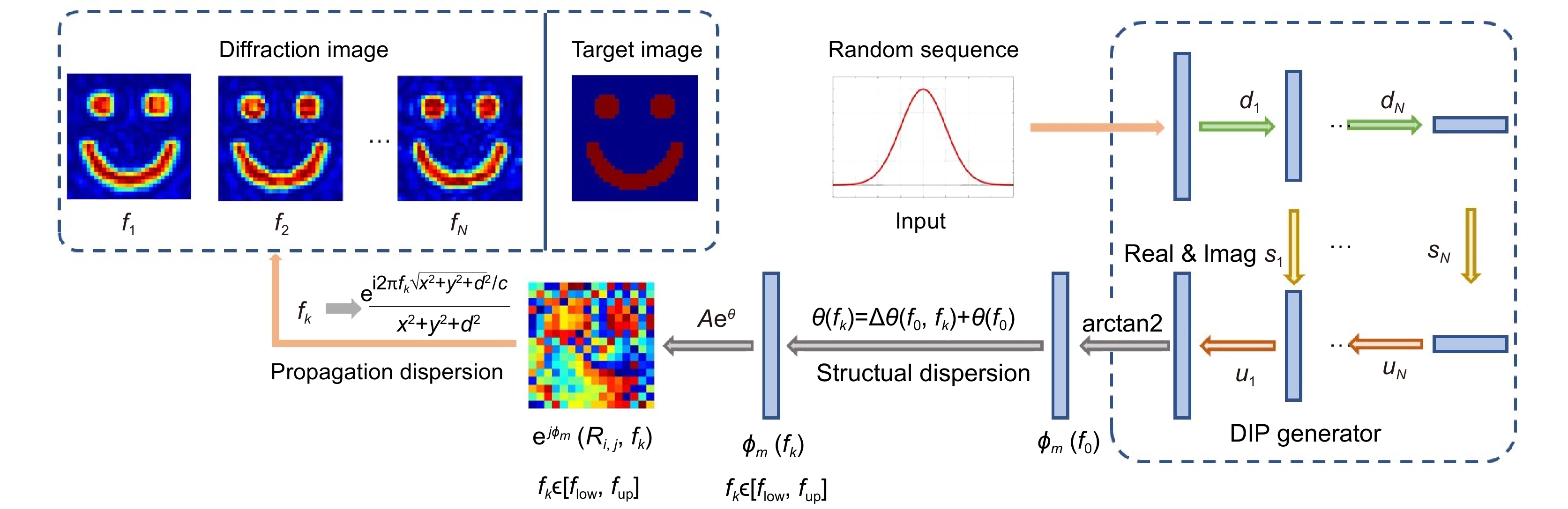
Overview: Computational holography digitizes the whole holographic process by computer, which greatly improves the accuracy and flexibility of imaging. It can realize the display of real or virtual objects without the limitation of the light source, which significantly expands the application field of holography. Metasurface is a two-dimensional planar form of metamaterial, which further increases the degree of freedom by introducing the concept of “macroscopic order” based on the use of structural parameters to control electromagnetic waves, and has the advantages of low material loss and simple processing. Due to its excellent modulation properties, the matesurface is well suitable as a wavefront encoding material for computing holograms, and the combination of metasurface and holographic imaging technology has become one of the current research hotspots in nanotechnology and electromagnetics. However, there are still problems such as low near-field imaging efficiency and narrow frequency band in the metasurface holographic imaging to restrict the practicalization of the metasurface holographic imaging. Aiming at the above problems, a design method of an achromatic broadband metasurface holographic imaging device based on Depth Image Prior (DIP) is proposed in this paper. Firstly, the phase feature vector of the central operating frequency is generated by the convolutional neural networks. Based on the structural dispersion of the actual metasurface elements, the phase feature vector in the working frequency band is also generated. Finally, the frequency band reconstruction image is generated by Rayley-Sommerfeld. The holographic phase map is obtained by the output of the deep convolutional neural network. High-quality reconstructed images can be generated after 20,000 iterations. The reflection cross-polarization unit is used as an example to verify the theoretical algorithm model in this paper. The holographic phase diagram of the network output was discretized at intervals of 10°, and MATLAB and CST co-simulation were used for rapid modeling. Numerical simulation results prove that the designed holographic imaging device can achieve a good achromatic imaging effect in the 9 GHz~11 GHz frequency band. The near-field measured results of bare object and cloak with a wideband frequency signal (8 GHz ~ 12 GHz) via Vector Network Analyzer (VNA) at 9 GHz, 9.5 GHz, 10 GHz, 10.5 GHz, and 11 GHz by plane wave illumination. The difference between experimental results and numerical simulation results is mainly caused by experimental errors and PCB machining errors. In general, relatively clear imaging can be observed in the design bandwidth range of 9 GHz~11 GHz. It has great potential applications in the field of holographic imaging and broadband functional device design.
-

-
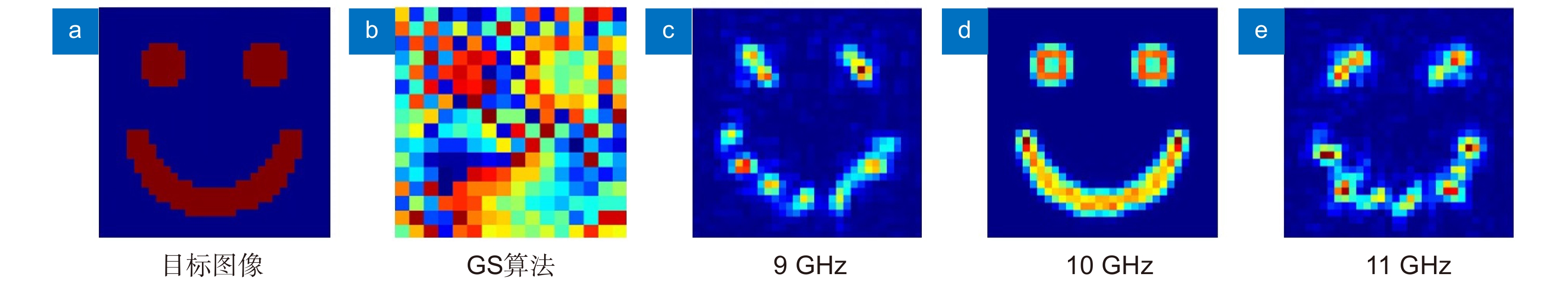
图 1 色散效应对成像器件的影响。(a) 成像目标;(b) 全息相位分布;(c-e) 9 GHz, 10 GHz, 11 GHz的重建像
Figure 1. Dispersion effects on imaging devices. (a) Imaging targets; (b) Holographic phase distribution; (c-e) Reconstruction images at 9 GHz, 10 GHz, and 11 GHz

图 2 基于深度图像先验(DIP)的宽频消色散超表面全息成像网络模型结构
Figure 2. A broadband dispersion metasurface holographic imaging network model based on the depth image priors (DIP)

图 3 网络训练过程。(a) 网络训练Loss值随迭代次数的变化;(b)不同迭代次数下网络输出的数值重建像
Figure 3. Network training process. (a) The change of network training loss value with the number of iterations; (b) Numerical reconstruction image outputs by the network under different iterations
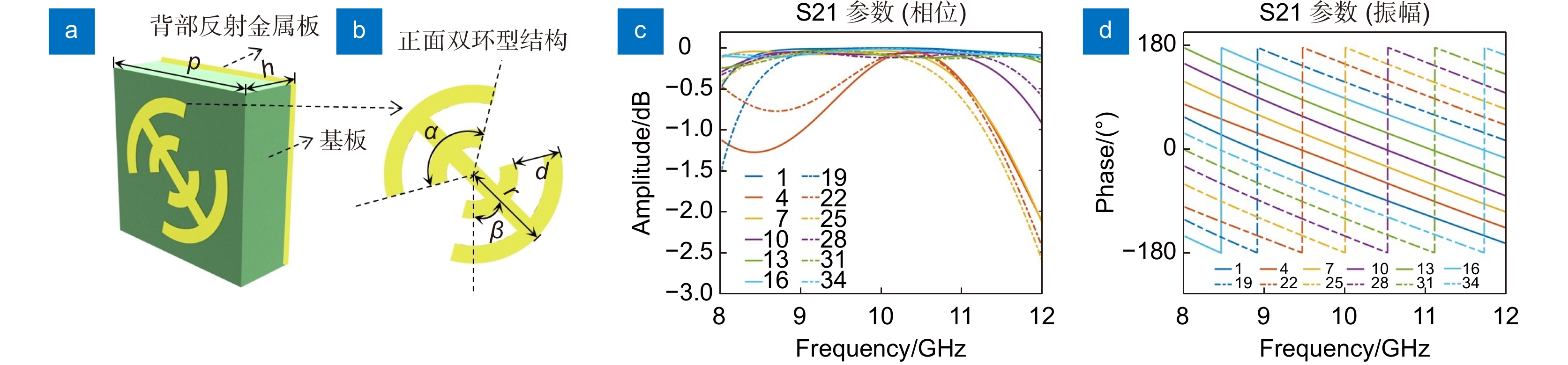
图 4 反射型交叉极化旋转超表面的单元结构。(a) 交叉极化转化单元的三维示意图;(b) 顶层金属结构;(c)和(d) 单元的极化转化效率和相位
Figure 4. Reflective cross-polarized rotational metasurface element. (a) Three-dimensional schematic diagram of the cross-polarization conversion unit; (b) Top-floor metal structure; (c) and (d) Polarization conversion efficiency and phase

图 5 宽频消色散超表面全息成像器件在150 mm处数值模拟仿真的电场强度分布图
Figure 5. Electric field intensity distributions of broadband dispersion metasurface holographic imaging device at 150 mm

图 6 宽频消色散超表面全息成像器件在150 mm处实验测试的电场强度分布图
Figure 6. Distributions of electric field intensity experimentally measured by a broadband dispersion metasurface holographic imaging device at 150 mm
表 1 不同超表面单元的结构参数和反射相位
Table 1. Structural parameters and reflected phases of different elements
单元序号 开口环角度α/(°) 开口环倾斜角度β/(°) 外环半径r/mm 内环半径(r−d)/mm 相位/(°) 9 GHz 10 GHz 11 GHz 1 82 45 3.6 1.6 5.32 −60.68 112.63 2 73 45 3.6 1.6 5.79 −49.91 101.65 3 64 45 3.6 1.6 16.82 −39.63 91.43 4 157 −45 4.16 2.16 25.56 −28.75 83.46 5 157 −45 4.02 2.02 35.41 −19.46 74.09 6 157 −45 3.88 1.88 45.82 −10.04 64.85 7 157 −45 3.74 1.74 57.70 0.42 54.89 8 157 −45 3.6 1.6 70.00 11.04 45.12 9 151 −45 3.6 1.6 77.51 19.07 36.65 10 145 −45 3.6 1.6 87.76 29.59 25.60 11 138 −45 3.6 1.6 98.48 40.51 14.18 12 131 −45 3.6 1.6 107.35 49.66 4.56 13 125 −45 3.6 1.6 116.53 59.03 5.10 14 118 −45 3.6 1.6 127.03 69.80 16.11 15 112 −45 3.6 1.6 136.64 79.79 26.31 16 104 −45 3.6 1.6 147.56 91.23 38.08 17 98 −45 3.6 1.6 154.69 98.74 45.95 18 90 −45 3.6 1.6 164.79 109.25 56.89 19 82 −45 3.6 1.6 174.90 119.50 67.52 20 73 −45 3.6 1.6 174.08 130.20 78.45 21 64 −45 3.6 1.6 163.15 140.39 88.57 22 157 45 4.16 2.16 154.45 151.21 96.47 23 157 45 4.02 2.02 144.55 160.58 105.95 24 157 45 3.88 1.88 135.05 169.00 114.11 25 157 45 3.74 1.74 122.31 179.61 125.10 26 157 45 3.6 1.6 110.35 169.25 134.58 27 151 45 3.6 1.6 101.29 159.76 144.55 28 145 45 3.6 1.6 92.15 150.35 154.44 29 138 45 3.6 1.6 81.42 139.42 165.89 30 131 45 3.6 1.6 71.08 128.84 176.88 31 125 45 3.6 1.6 62.21 119.76 173.76 32 118 45 3.6 1.6 53.21 110.40 164.06 33 112 45 3.6 1.6 43.55 100.34 153.77 34 104 45 3.6 1.6 32.53 88.80 141.89 35 98 45 3.6 1.6 24.53 80.41 133.19 36 90 45 3.6 1.6 15.17 70.73 123.09  下载: 导出CSV
-
[1] Gabor D. A new microscopic principle[J]. Nature, 1948, 161(4098): 777−778. doi: 10.1038/161777a0
[2] Brown B R, Lohmann A W. Complex spatial filtering with binary masks[J]. Appl Opt, 1966, 5(6): 967−969. doi: 10.1364/AO.5.000967
[3] Gabor D. Holography, 1948–1971[J]. Science, 1972, 177(4046): 299−313. doi: 10.1126/science.177.4046.299
[4] Jahani S, Jacob Z. All-dielectric metamaterials[J]. Nat Nanotechnol, 2016, 11(1): 23−36. doi: 10.1038/nnano.2015.304
[5] Zheng X Y, Smith W, Jackson J, et al. Multiscale metallic metamaterials[J]. Nat Mater, 2016, 15(10): 1100−1106. doi: 10.1038/nmat4694
[6] Valentine J, Zhang S, Zentgraf T, et al. Three-dimensional optical metamaterial with a negative refractive index[J]. Nature, 2008, 455(7211): 376−379. doi: 10.1038/nature07247
[7] Gansel J K, Thiel M, Rill M S, et al. Gold helix photonic metamaterial as broadband circular polarizer[J]. Science, 2009, 325(5947): 1513−1515. doi: 10.1126/science.1177031
[8] Ye W M, Zeuner F, Li X, et al. Spin and wavelength multiplexed nonlinear metasurface holography[J]. Nat Commun, 2016, 7: 11930. doi: 10.1038/ncomms11930
[9] Wang Q, Rogers E T F, Gholipour B, et al. Optically reconfigurable metasurfaces and photonic devices based on phase change materials[J]. Nat Photonics, 2016, 10(1): 60−65. doi: 10.1038/nphoton.2015.247
[10] Arbabi A, Horie Y, Bagheri M, et al. Dielectric metasurfaces for complete control of phase and polarization with subwavelength spatial resolution and high transmission[J]. Nat Nanotechnol, 2015, 10(11): 937−943. doi: 10.1038/nnano.2015.186
[11] Yu N F, Genevet P, Kats M A, et al. Light propagation with phase discontinuities: generalized laws of reflection and refraction[J]. Science, 2011, 334(6054): 333−337. doi: 10.1126/science.1210713
[12] Berry M V. Quantal phase factors accompanying adiabatic changes[J]. Proc R Soc Lond A Math Phys Sci, 1984, 392(1802): 45−57. doi: 10.1098/rspa.1984.0023
[13] Huang L L, Chen X Z, Mühlenbernd H, et al. Three-dimensional optical holography using a plasmonic metasurface[J]. Nat Commun, 2013, 4: 2808. doi: 10.1038/ncomms3808
[14] Yue Z J, Xue G L, Liu J, et al. Nanometric holograms based on a topological insulator material[J]. Nat Commun, 2017, 8: 15354. doi: 10.1038/ncomms15354
[15] Li L L, Cui T J, Ji W, et al. Electromagnetic reprogrammable coding-metasurface holograms[J]. Nat Commun, 2017, 8(1): 197. doi: 10.1038/s41467-017-00164-9
[16] Malek S C, Ee H S, Agarwal R. Strain multiplexed metasurface holograms on a stretchable substrate[J]. Nano Lett, 2017, 17(6): 3641−3645. doi: 10.1021/acs.nanolett.7b00807
[17] Chen T H, Li J, Cai T, et al. Design of a reconfigurable broadband greyscale multiplexed metasurface hologram[J]. Appl Opt, 2020, 59(12): 3660−3665. doi: 10.1364/AO.386811
[18] Genevet P, Capasso F. Holographic optical metasurfaces: a review of current progress[J]. Rep Prog Phys, 2015, 78(2): 024401. doi: 10.1088/0034-4885/78/2/024401
[19] 许可, 王星儿, 范旭浩, 等. 超表面全息术: 从概念到实现[J]. 光电工程, 2022, 49(10): 220183. doi: 10.12086/oee.2022.220183
Xu K, Wang X E, Fan X H, et al. Meta-holography: from concept to realization[J]. Opto-Electron Eng, 2022, 49(10): 220183. doi: 10.12086/oee.2022.220183
[20] 杨睿, 于千茜, 潘一苇, 等. 基于片上超表面的多路方向复用全息术[J]. 光电工程, 2022, 49(10): 220177. doi: 10.12086/oee.2022.220177
Yang R, Yu Q Q, Pan Y W, et al. Directional-multiplexing holography by on-chip metasurface[J]. Opto-Electron Eng, 2022, 49(10): 220177. doi: 10.12086/oee.2022.220177
[21] Gao H, Fan X H, Xiong W, et al. Recent advances in optical dynamic meta-holography[J]. Opto-Electron Adv, 2021, 4(11): 210030. doi: 10.29026/oea.2021.210030
[22] Li X, Chen Q M, Zhang X, et al. Time-sequential color code division multiplexing holographic display with metasurface[J]. Opto-Electron Adv, 2023, 6: 220060. doi: 10.29026/oea.2023.220060
[23] Li G, Lee D, Jeong Y, et al. Holographic display for see-through augmented reality using mirror-lens holographic optical element[J]. Opt Lett, 2016, 41(11): 2486−2489. doi: 10.1364/OL.41.002486
[24] Zimin V, Hussain F. High-aperture raster holography for particle imaging[J]. Opt Lett, 1994, 19(15): 1158−1160. doi: 10.1364/OL.19.001158
[25] Lempitsky V, Vedaldi A, Ulyanov D. Deep image prior[C]//Proceedings of 2018 IEEE/CVF Conference on Computer Vision and Pattern Recognition, 2018: 9446–9454. https://doi.org/10.1109/CVPR.2018.00984.
-
 点击扫一扫
点击扫一扫
图(7)
表(1)
计量
- 文章访问数: 2051
- PDF下载数: 404
- 施引文献: 0


