
 E-mail Alert
 RSS
RSS
Switchable edge detection and imaging based on a phase-change metasurface with Ge2Sb2Se4Te1
-
摘要
本文提出了一种在不借助4f成像系统的情况下实现可切换边缘检测与聚焦成像的超表面。超表面由相变材料(Ge2Sb2Se4Te1,GSST)方柱和硅(Si)基底组成的单元结构周期性排列而成。其不同功能的实现来源于GSST处于非晶态和晶态下所提供的不同传输相位与几何相位的优化组合。当GSST处于非晶态和晶态下,单元结构平均交叉偏振透射系数分别在0.77和0.42以上。为了验证设计的可行性,本文对所设计的可切换超表面在晶态和非晶态下分别进行了仿真与理论计算,表现出优异的成像与边缘检测效果。所提出的超表面及其工作原理在生物医学成像和缺陷检测等领域有潜在应用价值。
Abstract
A versatile metasurface platform based on phase change materials (PCMs) is provided to realize dynamic switching between edge detection and imaging without the assistance of a 4f imaging system. The metasurface consists of a periodic arrangement of unit structures which consists of a Ge2Sb2Se4Te1(GSST) nanofin on a silicon substrate. The dynamically switchable performance results from the combination of the geometric phase and two independent propagation phases that are provided by the composed phase-change material meta-atoms in amorphous and crystalline states. The average cross-polarized transmission coefficients are 0.77 and 0.42 in the amorphous and crystalline states. In order to verify the feasibility of the design, simulation and theoretical calculation of the designed switchable metasurface are carried out in crystalline state and amorphous state respectively, which show excellent imaging and edge detection results. The proposed metasurface and its working principle have potential applications in biomedical imaging and defect detection.ect detection.
-
Key words:
- edge detection /
- imaging /
- phase change material /
- metasurface
-
Overview
Overview: This paper is devoted to the research of switchable edge detection and imaging metasurface without a 4f system. Edge detection and imaging both are important parts of modern imaging processing, which are widely applied in the fields of robot vision, modern artificial intelligence, and medical imaging operation. The method of processing images based on mathematical operations usually has low operational speed and high-power consumption. Therefore, optical analog computation is suggested to operate image processing performs by manipulating optical signal carrying image information. Optical analog computation based on the traditional optical system needs bulky configurations which is improper in highly integrated modern optical systems. Therefore, this paper analyzes and designs the phase distribution which enable switchable edge detection and imaging and proved the feasibility of the design by operating simulation and theoretical calculation with the proposed metasurface. The switchable ability relies on the switchable photonic spin-orbit interactions (SOIs). Therefore, firstly this paper described and analyzed SOIs. And then we utilize two optical properties of GSST in crystalline and amorphous states to design eight unit cells which have different phases when GSST is in different states. In order to prove that the switchable SOIs can be realized by using the free combination of the proposed eight unit cells, the gradient metasurface consists of unit cells designed to perform symmetric photonic SOIs when GSST is in the amorphous state, resulting in symmetric refractive angles -17.1° and 17.1° for LCP and RCP incidence. While the designed gradient metasurface performs asymmetric photonic SOIs when GSST is in the crystalline state, resulting in refractive angles of 0° and 32° for LCP and RCP incidence. The simulated refractive angles are approximately-19.5°, 17.7° and 0°, 31.2° in the amorphous and crystalline state. The highly consistent results between simulation and theoretical calculation prove the feasibility of this design. Then the principle of imaging and edge detection is analyzed theoretically, and by analyzing and optimizing legitimately, designed the propagation phase at the crystalline state and orientation angle for the unit cells. Employing this design method, when GSST is in the amorphous state the phase of transmitted LCP light fulfills the focusing phase. When GSST is in the crystalline state, the transmitted wavefronts of LCP and RCP can match the phase distributions of edge detection. Further, in order to prove the feasibility of the designed metasurface, a metasurface model is created to operate edge detection and imaging in CST Microwave Studio. The edge imaging of the object and the object imaging in simulated results proved the feasibility of the designed metasurface. Finally, at the same time, the letters "S I C N U" and the sun and immortal birds are chosen as objects for calculating the imaging of complex objects theoretically under the above-mentioned phase distributions. The theoretic edge imaging and imaging of the letters "S I C N U" and the sun and immortal birds proved that designed two-phase distributions can realize edge detection and bright-field imaging well. To sum up, the metasurface designed in this paper can provide a kind of design without a 4f system to realize switchable edge detection and imaging.
-

-
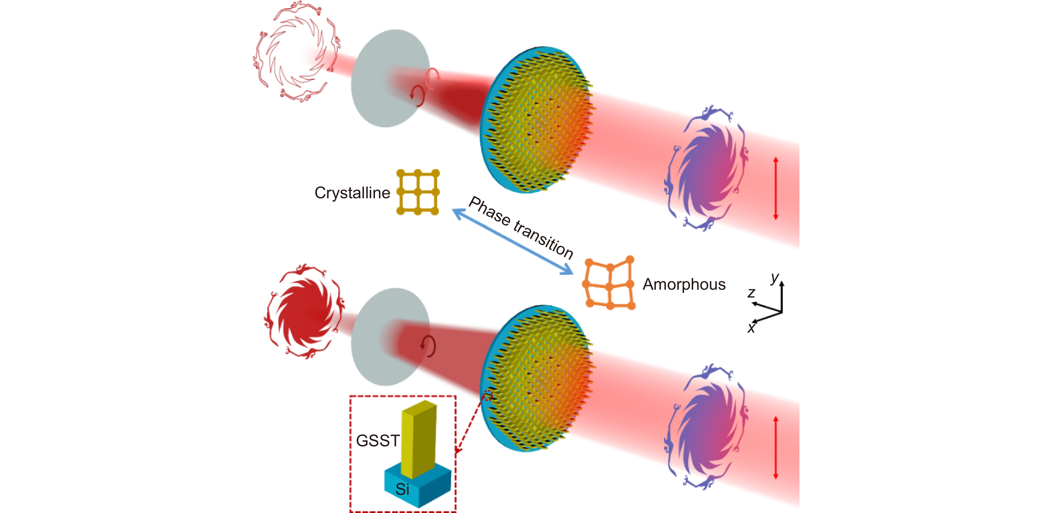
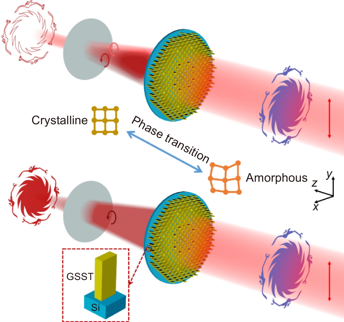
图 1 基于GSST相变实现边缘检测和聚焦成像间动态切换的超表面原理图
Figure 1. Schematic of the metasurface platform enables dynamic switching between the edge detection and imaging based on the phase transition of GSST

图 2 (a, b) 不同视图下的单元结构示意图;(c, d) 10.6 μm波长下八个单元结构的相位响应和交叉偏振系数。方柱结构和基底的材料分别是GSST和Si。恒定参数(高度、周期):H = 6 μm, P = 4 μm;八个单元结构的长度(L)和宽度(W)分别为L= 2.9 μm,3.0 μm,3.3 μm,3.2 μm,3.5 μm,3.79 μm,3.82 μm和2.68 μm,W= 1.34 μm,1.28 μm,1.2 μm,1.14 μm,1.0 μm,0.83 μm,0.8 μm和1.41 μm
Figure 2. (a, b) Schematic illustrations of unit cells at different views. (c, d) Simulated phase responses and cross-polarized coefficients of eight unit cells for circularly polarized light at the wavelength of 10.6 μm. The materials of nanofins and substrate are GSST and Si, respectively. Constant parameters: H = 6 μm, P = 4 μm. The length (L) and width (W) of eight unit cells are L= 2.9, 3.0, 3.3, 3.2, 3.5, 3.79, 3.82 and 2.68 μm, W= 1.34, 1.28, 1.2, 1.14, 1.0, 0.83, 0.8 and 1.41 μm
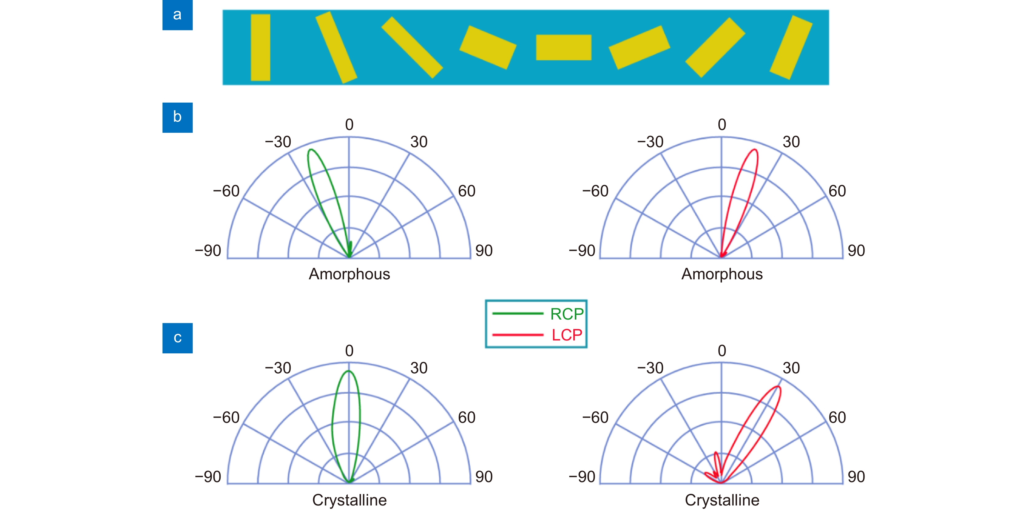
图 3 (a) 可调谐异常透射梯度超表面周期结构示意图;(b) a-GSST下的模拟交叉偏振远场分布;(c) c-GSST下的模拟交叉偏振远场分布
Figure 3. (a) Schematic illustration of a periodic gradient metasurface for tunable anomalous transmission; (b) The simulated cross-polarized far-field distributions when GSST is amorphous; (c) The simulated cross-polarized far-field distributions when GSST is crystalline
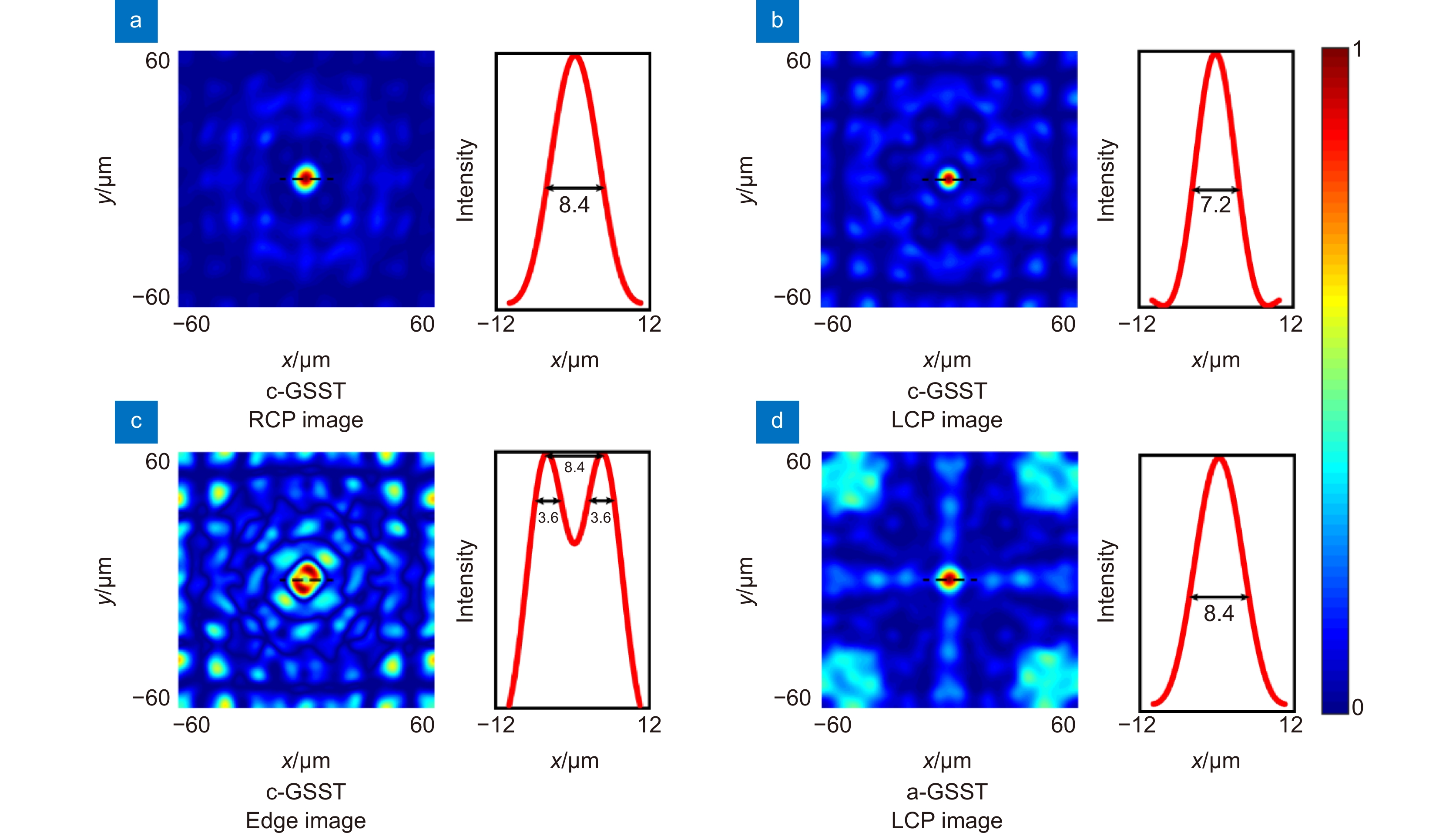
图 4 入射光为10.6 μm时GSST不同态下像面强度分布。(a) c-GSST下,z=100 μm时模拟RCP成像强度分布和中心虚线部分归一化强度分布;(b) c-GSST下,z=100 μm时模拟LCP成像强度分布和中心虚线部分归一化强度分布;(c) c-GSST下,z=100 μm时模拟偏振滤波后的像面强度分布和中心虚线部分归一化强度分布;(d) a-GSST下,z=1000 μm时模拟聚焦成像强度分布和中心虚线部分归一化强度分布
Figure 4. The simulated image intensity distributions of different states under the 10.6 μm incident beam. (a) The simulated RCP image intensity distributions and normalized intensity distributions of the dotted line on z=100 μm plane when GSST is crystalline; (b) The simulated LCP image intensity distributions and normalized intensity distributions of the dotted line on z=100 μm plane when GSST is crystalline; (c) The simulated edge image intensity distribution and normalized intensity distributions of the dotted line on z=100 μm plane when GSST is crystalline; (d) The simulated LCP image intensity distribution and normalized intensity distributions of the dotted line on z=1000 μm plane when GSST is amorphousSST is amorphous
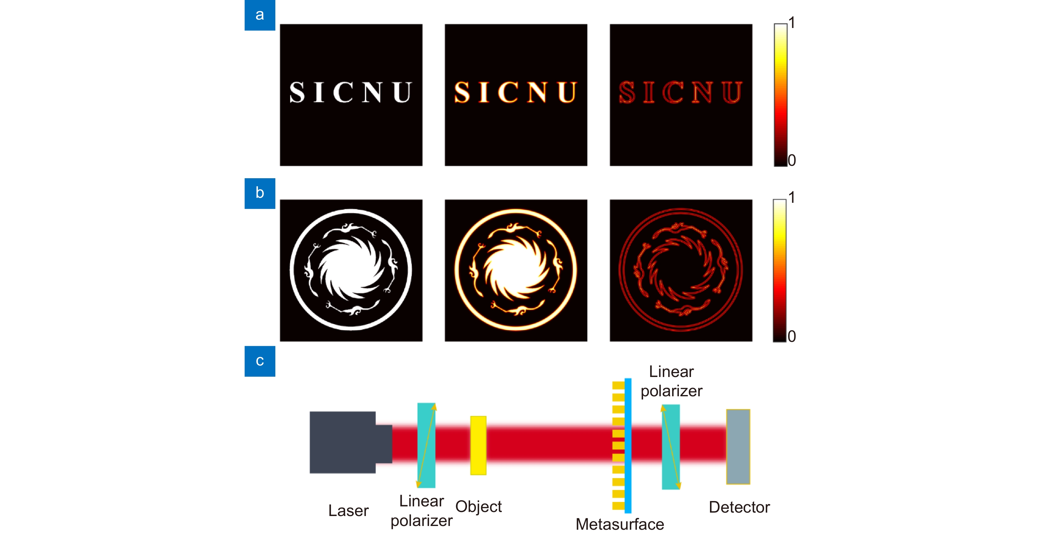
图 5 (a) 理论模拟计算成像物体为“S I C N U”字母时,从左到右依次为:物体图像,聚焦成像,边缘检测成像; (b) 理论模拟计算成像物体为太阳神鸟时,从左到右依次为:物体图像,聚焦成像,边缘检测成像;(c) 图像处理系统示意图
Figure 5. (a) The calculation results when the object is "S I C N U", from left to right: object image, imaging, edge detection imaging; (b) The calculation results when the object is the sun and immortal birds, from left to right: object image, imaging, and edge detection imaging; (c) Schematic illustration of the system for image processing
-
参考文献
[1] Kwon H, Sounas D, Cordaro A, et al. Nonlocal metasurfaces for optical signal processing[J]. Phys Rev Lett, 2018, 121(17): 173004. doi: 10.1103/PhysRevLett.121.173004
[2] Davis T J, Eftekhari F, Gómez D E, et al. Metasurfaces with asymmetric optical transfer functions for optical signal processing[J]. Phys Rev Lett, 2019, 123(1): 013901. doi: 10.1103/PhysRevLett.123.013901
[3] Solli D R, Jalali B. Analog optical computing[J]. Nat Photonics, 2015, 9(11): 704−706. doi: 10.1038/nphoton.2015.208
[4] Zhu T F, Lou Y J, Zhou Y H, et al. Generalized spatial differentiation from the spin hall effect of light and its application in image processing of edge detection[J]. Phys Rev Appl, 2019, 11(3): 034043. doi: 10.1103/PhysRevApplied.11.034043
[5] Mueller J P B, Rubin N A, Devlin R C, et al. Metasurface polarization optics: independent phase control of arbitrary orthogonal states of polarization[J]. Phys Rev Lett, 2017, 118(11): 113901. doi: 10.1103/PhysRevLett.118.113901
[6] Chen W T, Zhu A Y, Capasso F. Flat optics with dispersion-engineered metasurfaces[J]. Nat Rev Mater, 2020, 5(8): 604−620. doi: 10.1038/s41578-020-0203-3
[7] Huang Y J, Xiao T X, Xie Z W, et al. Single-layered phase-change metasurfaces achieving efficient wavefront manipulation and reversible chiral transmission[J]. Opt Express, 2022, 30(2): 1337−1350. doi: 10.1364/OE.447545
[8] Huang Y J, Xiao T X, Xie Z W, et al. Multistate nonvolatile metamirrors with tunable optical chirality[J]. ACS Appl Mater Interfaces, 2021, 13(38): 45890−45897. doi: 10.1021/acsami.1c14204
[9] Huang Y J, Xiao T X, Xie Z W, et al. Single-layered reflective metasurface achieving simultaneous spin-selective perfect absorption and efficient wavefront manipulation[J]. Adv Opt Mater, 2021, 9(5): 2001663. doi: 10.1002/adom.202001663
[10] Zhang Y X, Pu M B, Jin J J, et al. Crosstalk-free achromatic full Stokes imaging polarimetry metasurface enabled by polarization-dependent phase optimization[J]. Opto-Electron Adv, 2022, 5(11): 220058. doi: 10.29026/oea.2022.220058
[11] Li J T, Wang G C, Yue Z, et al. Dynamic phase assembled terahertz metalens for reversible conversion between linear polarization and arbitrary circular polarization[J]. Opto-Electron Adv, 2022, 5(1): 210062. doi: 10.29026/oea.2022.210062
[12] Wang Y L, Fan Q B, Xu T. Design of high efficiency achromatic metalens with large operation bandwidth using bilayer architecture[J]. Opto-Electron Adv, 2021, 4(1): 200008. doi: 10.29026/oea.2021.200008
[13] Yue Z, Li J T, Li J, et al. Terahertz metasurface zone plates with arbitrary polarizations to a fixed polarization conversion[J]. Opto-Electron Sci, 2022, 1(3): 210014. doi: 10.29026/oes.2022.210014
[14] 蓝翔, 邓钦荣, 张汶婷, 等. 基于扭转悬链线结构的高效手性吸波器[J]. 光电工程, 2022, 49(10): 220157. doi: 10.12086/oee.2022.220157
Lan X, Deng Q R, Zhang W T, et al. Efficient chiral absorber based on twisted catenary structure[J]. Opto-Electron Eng, 2022, 49(10): 220157. doi: 10.12086/oee.2022.220157
[15] 杨睿, 于千茜, 潘一苇, 等. 基于片上超表面的多路方向复用全息术[J]. 光电工程, 2022, 49(10): 220177. doi: 10.12086/oee.2022.220177
Yang R, Yu Q Q, Pan Y W, et al. Directional-multiplexing holography by on-chip metasurface[J]. Opto-Electron Eng, 2022, 49(10): 220177. doi: 10.12086/oee.2022.220177
[16] Huang Y J, Xiao T X, Chen S, et al. All-optical controlled-NOT logic gate achieving directional asymmetric transmission based on metasurface doublet[J]. Opto-Electron Adv, 2023, 6: 220073. doi: 10.29026/oea.2023.220073
[17] Zheng G X, Mühlenbernd H, Kenney M, et al. Metasurface holograms reaching 80% efficiency[J]. Nat Nanotechnol, 2015, 10(4): 308−312. doi: 10.1038/nnano.2015.2
[18] Li X, Chen L W, Li Y, et al. Multicolor 3D meta-holography by broadband plasmonic modulation[J]. Sci Adv, 2016, 2(11): e1601102. doi: 10.1126/sciadv.1601102
[19] Xie X, Liu K P, Pu M B, et al. All-metallic geometric metasurfaces for broadband and high-efficiency wavefront manipulation[J]. Nanophotonics, 2020, 9(10): 3209−3215. doi: 10.1515/nanoph-2019-0415
[20] Tang Z Y, Li L, Zhang H C, et al. Multifunctional Janus metasurfaces achieving arbitrary wavefront manipulation at dual frequency[J]. Mater Des, 2022, 223: 111264. doi: 10.1016/j.matdes.2022.111264
[21] 许可, 王星儿, 范旭浩, 等. 超表面全息术: 从概念到实现[J]. 光电工程, 2022, 49(10): 220183. doi: 10.12086/oee.2022.220183
Xu K, Wang X E, Fan X H, et al. Meta-holography: from concept to realization[J]. Opto-Electron Eng, 2022, 49(10): 220183. doi: 10.12086/oee.2022.220183
[22] Devlin R C, Ambrosio A, Rubin N A, et al. Arbitrary spin-to–orbital angular momentum conversion of light[J]. Science, 2017, 358(6365): 896−901. doi: 10.1126/science.aao5392
[23] Li Q T, Dong F L, Wang B, et al. Free-space optical beam tapping with an all-silica metasurface[J]. ACS Photonics, 2017, 4(10): 2544−2549. doi: 10.1021/acsphotonics.7b00812
[24] Chen W T, Zhu A Y, Sanjeev V, et al. A broadband achromatic metalens for focusing and imaging in the visible[J]. Nat Nanotechnol, 2018, 13(3): 220−226. doi: 10.1038/s41565-017-0034-6
[25] Wang S M, Wu P C, Su V C, et al. A broadband achromatic metalens in the visible[J]. Nat Nanotechnol, 2018, 13(3): 227−232. doi: 10.1038/s41565-017-0052-4
[26] Cai W S, Chettiar U K, Kildishev A V, et al. Optical cloaking with metamaterials[J]. Nat Photonics, 2007, 1(4): 224−227. doi: 10.1038/nphoton.2007.28
[27] Xie X, Li X, Pu M B, et al. Plasmonic metasurfaces for simultaneous thermal infrared invisibility and holographic illusion[J]. Adv Funct Mater, 2018, 28(14): 1706673. doi: 10.1002/adfm.201706673
[28] Zhou Y, Wu W H, Chen R, et al. Analog optical spatial differentiators based on dielectric metasurfaces[J]. Adv Opt Mater, 2020, 8(4): 1901523. doi: 10.1002/adom.201901523
[29] Cordaro A, Kwon H, Sounas D, et al. High-index dielectric metasurfaces performing mathematical operations[J]. Nano Lett, 2019, 19(12): 8418−8423. doi: 10.1021/acs.nanolett.9b02477
[30] Dong Z W, Si J N, Yu X Y, et al. Optical spatial differentiator based on subwavelength high-contrast gratings[J]. Appl Phys Lett, 2018, 112(18): 181102. doi: 10.1063/1.5026309
[31] Zhou Y, Zheng H Y, Kravchenko I I, et al. Flat optics for image differentiation[J]. Nat Photonics, 2020, 14(5): 316−323. doi: 10.1038/s41566-020-0591-3
[32] Wan L, Pan D P, Yang S F, et al. Optical analog computing of spatial differentiation and edge detection with dielectric metasurfaces[J]. Opt Lett, 2020, 45(7): 2070−2073. doi: 10.1364/OL.386986
[33] Huo P C, Zhang C, Zhu W Q, et al. Photonic spin-multiplexing metasurface for switchable spiral phase contrast imaging[J]. Nano Lett, 2020, 20(4): 2791−2798. doi: 10.1021/acs.nanolett.0c00471
[34] He Q, Zhang F, Pu M B, et al. Monolithic metasurface spatial differentiator enabled by asymmetric photonic spin-orbit interactions[J]. Nanophotonics, 2021, 10(1): 741−748. doi: 10.1515/nanoph-2020-0366
[35] Shaltout A M, Shalaev V M, Brongersma M L. Spatiotemporal light control with active metasurfaces[J]. Science, 2019, 364(6441): eaat3100. doi: 10.1126/science.aat3100
[36] Chang C M, Chu C H, Tseng M L, et al. Local electrical characterization of laser-recorded phase-change marks on amorphous Ge2Sb2Te5 thin films[J]. Opt Express, 2011, 19(10): 9492−9504. doi: 10.1364/OE.19.009492
[37] Chen Y G, Kao T S, Ng B, et al. Hybrid phase-change plasmonic crystals for active tuning of lattice resonances[J]. Opt Express, 2013, 21(11): 13691−13698. doi: 10.1364/OE.21.013691
[38] Yamada N. Origin, secret, and application of the ideal phase-change material GeSbTe[J]. Phys Status Solidi, 2012, 249(10): 1837−1842. doi: 10.1002/pssb.201200618
[39] Loke D, Lee T H, Wang W J, et al. Breaking the speed limits of phase-change memory[J]. Science, 2012, 336(6088): 1566−1569. doi: 10.1126/science.1221561
[40] Michel A K U, Zalden P, Chigrin D N, et al. Reversible optical switching of infrared antenna resonances with ultrathin phase-change layers using femtosecond laser pulses[J]. ACS Photonics, 2014, 1(9): 833−839. doi: 10.1021/ph500121d
[41] Wang Q, Rogers E T F, Gholipour B, et al. Optically reconfigurable metasurfaces and photonic devices based on phase change materials[J]. Nat Photonics, 2016, 10(1): 60−65. doi: 10.1038/nphoton.2015.247
[42] Du K K, Li Q, Lyu Y B, et al. Control over emissivity of zero-static-power thermal emitters based on phase-changing material GST[J]. Light Sci Appl, 2017, 6(1): e16194. doi: 10.1038/lsa.2016.194
[43] Zhang Y F, Chou J B, Li J Y, et al. Broadband transparent optical phase change materials for high-performance nonvolatile photonics[J]. Nat Commun, 2019, 10(1): 4279. doi: 10.1038/s41467-019-12196-4
[44] Arbabi A, Horie Y, Bagheri M, et al. Dielectric metasurfaces for complete control of phase and polarization with subwavelength spatial resolution and high transmission[J]. Nat Nanotechnol, 2015, 10(11): 937−943. doi: 10.1038/nnano.2015.186
[45] Bliokh K Y, Rodríguez-Fortuño F J, Nori F, et al. Spin–orbit interactions of light[J]. Nat Photonics, 2015, 9(12): 796−808. doi: 10.1038/nphoton.2015.201
[46] Zhang F, Pu M B, Luo J, et al. Symmetry breaking of photonic spin‐orbit interactions in metasurfaces[J]. Opto-Electron Eng, 2017, 44(3): 319−325. doi: 10.3969/j.issn.1003-501X.2017.03.006
[47] Yang H, Xie Z W, He H R, et al. Switchable imaging between edge-enhanced and bright-field based on a phase-change metasurface[J]. Opt Lett, 2021, 46(15): 3741−3744. doi: 10.1364/OL.428870
[48] Zhou J X, Qian H L, Chen C F, et al. Optical edge detection based on high-efficiency dielectric metasurface[J]. Proc Natl Acad Sci USA, 2019, 116(23): 11137−11140. doi: 10.1073/pnas.1820636116
-
访问统计
 下载:
下载:
 点击扫一扫
点击扫一扫
图(6)
计量
- 文章访问数:
- PDF下载数:
- 施引文献: 0


