
 E-mail Alert
 RSS
RSS
-
摘要:
本文利用亚波长硅圆柱组成的超表面设计了用于太赫兹探测器的聚焦透镜,通过改变硅柱的直径,实现对太赫兹波传输相位0~2π的调控。在1 THz频率下,所设计的单面超表面透镜,太赫兹波电场能量密度提升到入射平面波的32倍。基于工艺制备可行性和抗反射考虑,提出了一种双面超表面透镜,将电场能量密度提升到入射平面波的44倍。对比于传统超半球太赫兹硅透镜,超表面透镜具有厚度薄,体积小的优点,有利于太赫兹探测器组件的小型化,为实现与太赫兹探测器的集成提供了可能性。
Abstract:In this paper, a focusing lens for terahertz detection is designed using a metasurface composed of sub-wavelength silicon cylinders. By tuning the diameter of the silicon cylinder, the transmission phase of the THz wave is controlled from 0 to 2π. At 1 THz, the terahertz electric field energy density focused by the single-sided metasurface lens designed can be increased to 32 times that of the incident wave. After adding the anti-reflection, a double-sided metasurface lens is proposed, which is feasible in processing, increasing the electric field energy density to 44 times that of the original. Compared with the traditional hyper-hemispheric terahertz silicon lenses, our metasurface lens has the advantages of thin thickness and small volume, which is conducive to the miniaturization of the terahertz detector component and provides the possibility to realize the integration with the terahertz detector.
-
Key words:
- metasurface /
- terahertz /
- focus
-
Overview: Terahertz detector is an important device in the field of terahertz technology, and it is important to improve its sensitivity. The sensitivity of the detector can be improved in two aspects: one is to further optimize the antenna of the detector, and the other is to optimize the size of the detector and the spot size of incident terahertz wave. Due to the long wavelength of the electromagnetic wave in the terahertz band, the spot size is much larger than the effective acceptance area of the detector, which limits the effective absorption rate of the detector to the incident terahertz wave. In order to make the focus spot to be small, the lens aperture needs to be increased. At present, the commonly used method is to integrate the hyper-hemispheric silicon lens with the terahertz detector to reduce the spot size by one order of magnitude and increase the electric field energy density. However, hyper-hemispheric silicon lens is difficult to be ultra-thin and ultra-light, and is not planar, which is not conducive to the device integration, especially for array detectors. In this paper, a series of metasurface lenses for terahertz detectors are designed using sub-wavelength silicon cylinders. By tuning the diameter of the silicon cylinders, the transmission phase of the terahertz wave can be controlled from 0 to 2π with high transmission amplitude. At 1 THz, the backside integration of the designed single-surface lens with the terahertz detector can increase the electric field energy density in the core region of the THz detector to 32 times that of the incident plane wave, and reduce the focal spot to the same order of magnitude as the wavelength. Based on the feasibility of fabrication and anti-reflection considerations, we propose a two-sided metasurface lens, which further increases the energy density of the electric field to 44 times that of the incident plane wave. Compared with the traditional hyper-hemispheric silicon lenses, the size and thickness of the metasurface lens are smaller and more convenient for integration. Metasurface lenses have a great prospect for reducing the complexity of the terahertz system and improving the responsiveness of the detector, and provide a new idea for the integration and miniaturization of the terahertz device. However, the current metasurface lenses produce many side lobes after focusing, resulting in low focusing efficiency. Further research needs to further optimize the materials and unit structures of the metasurface lenses, to improve the focusing efficiency and electric field energy density.
-

-

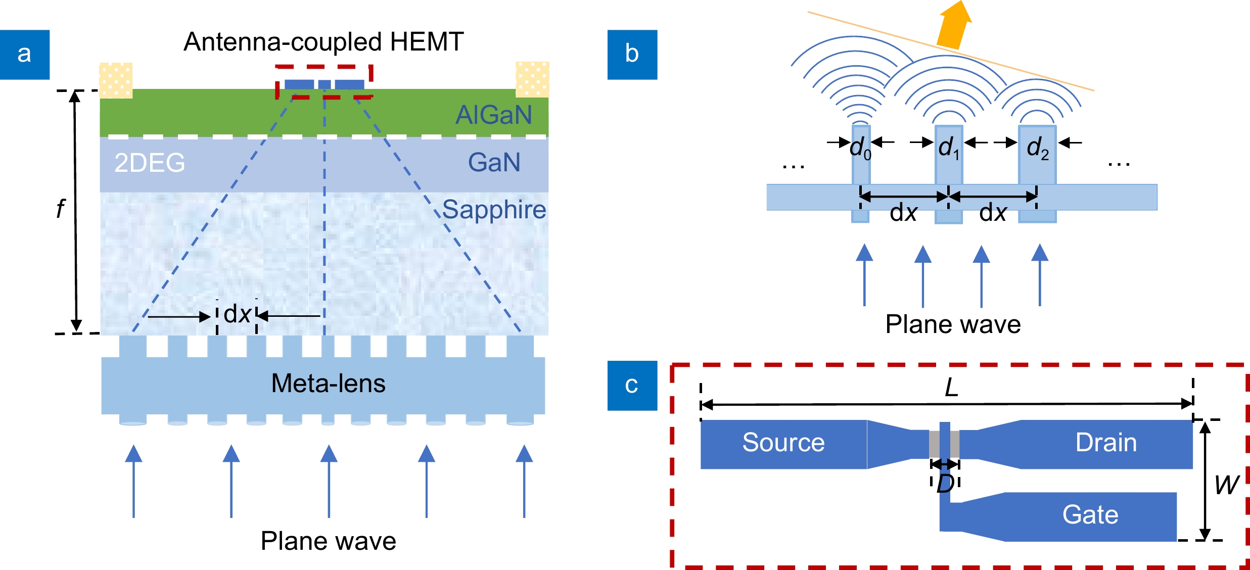
图 1 (a) AlGaN/GaN 太赫兹探测器与超表面透镜集成模型;(b) 超表面单元阵列的相位调控示意图;(c) 太赫兹天线结构示意图
Figure 1. (a) The integration model of an AlGaN/GaN terahertz detector and a metasurface lens; (b) Schematic diagram of phase regulation of metasurface element array; (c) Schematic diagram of terahertz antenna structure
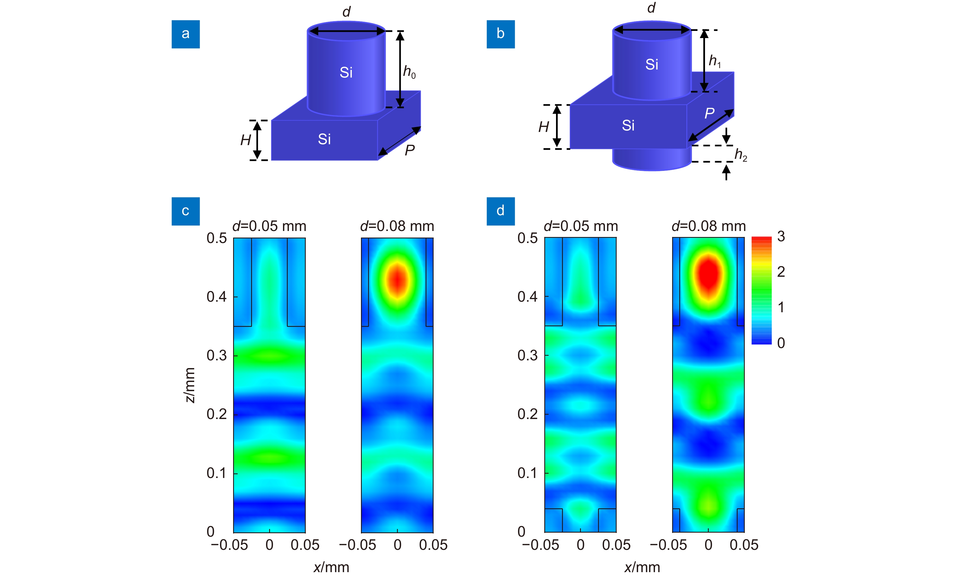
图 2 (a),(c) 分别为单面单元结构示意图及其能量分布;(b),(d) 分别为双面单元结构示意图及其能量分布
Figure 2. (a) and (c) show the schematic diagram of single-sided cell structure and its energy distribution; (b) and (d) show the schematic diagram of double-sided cell structure and its energy distribution
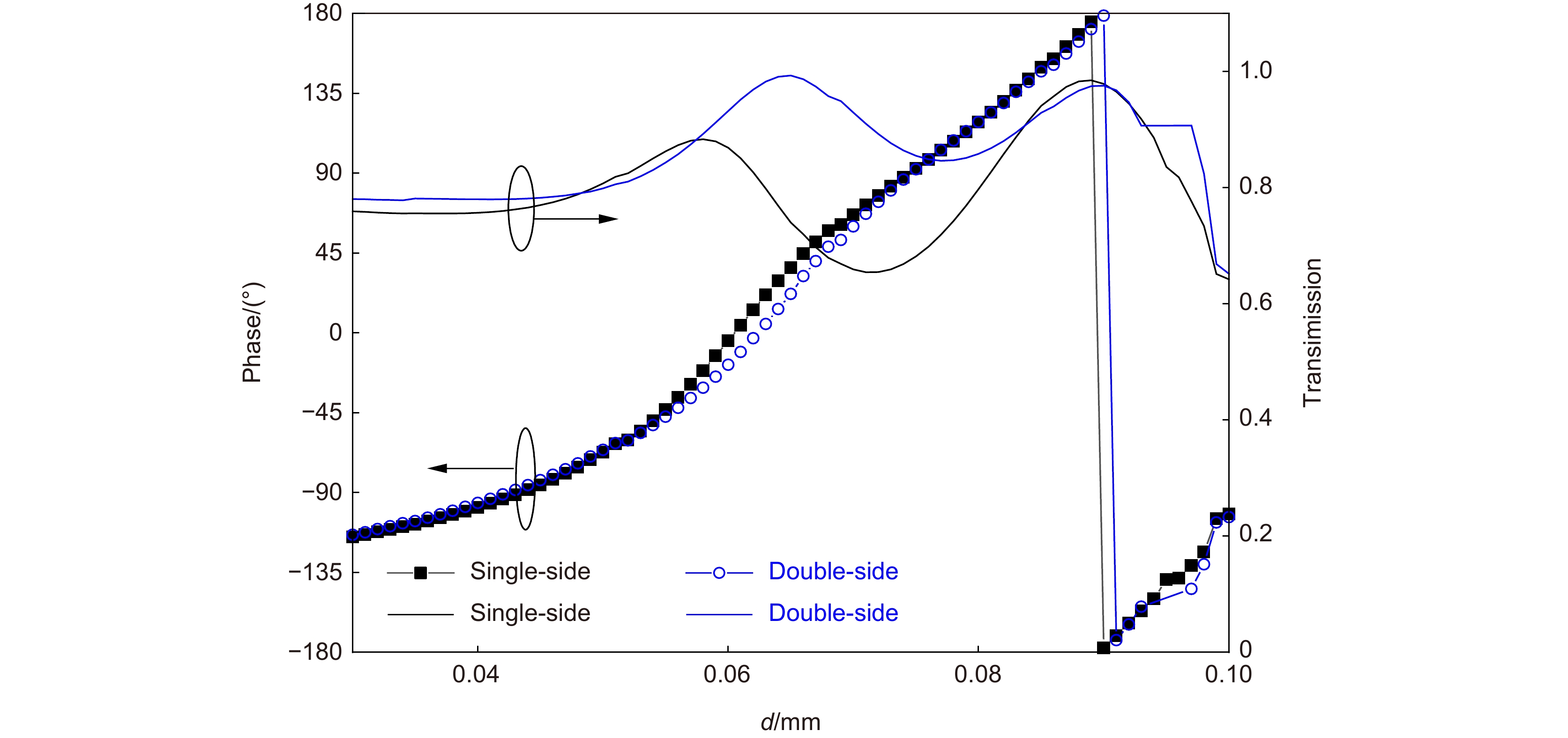
图 3 超表面透镜单双面结构的相位和透射率随直径变化曲线
Figure 3. The phase and transmittance curves of the single and double structure of metasurface lens vary with diameter
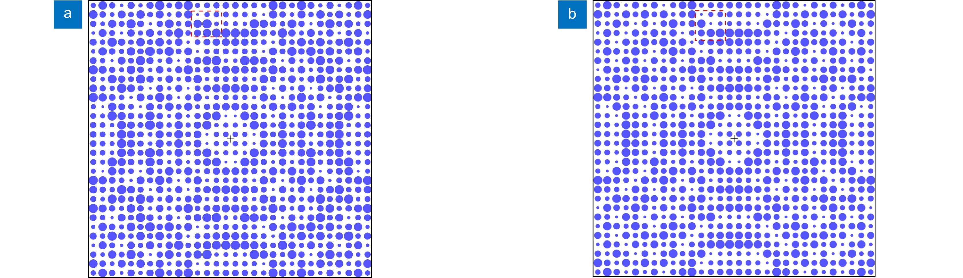
图 5 (a) 单面超表面透镜布阵;(b) 双面超表面透镜布阵
Figure 5. (a) The array of single-sided metasurface lens; (b) The array of double-sided metasurface lens
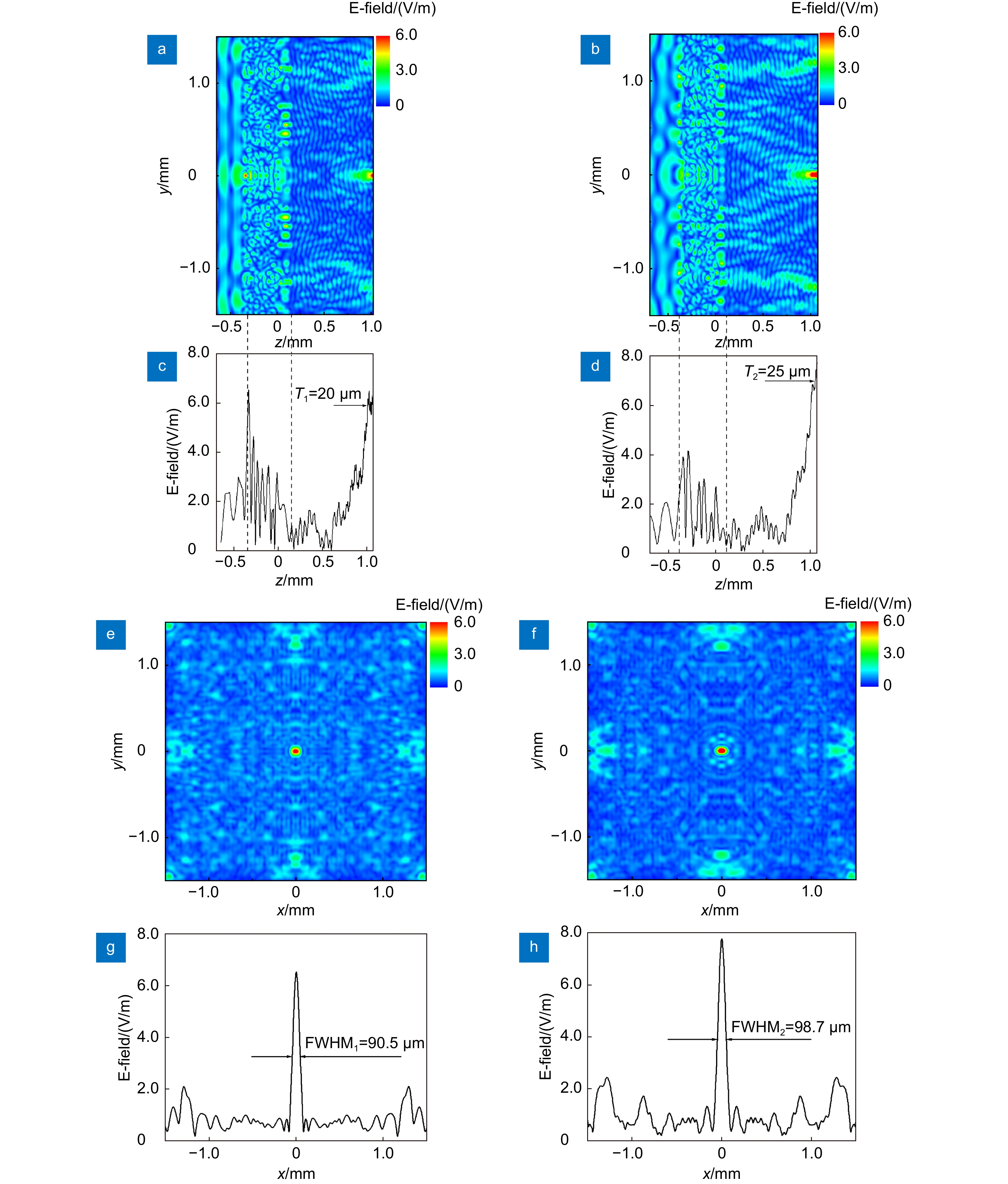
图 6 (a),(c) 分别为单面结构x=0时,y-z面场强分布和y=0时一维分布;(b),(d) 分别为双面结构超表面透镜x=0时,y-z面场强分布和y=0时一维分布;(e),(g) 分别为单面结构的超表面透镜z=1.026 mm时,x-y面场强分布和y=0时一维分布;(f),(h) 分别为双面结构的超表面透镜z=1.067 mm时,x-y面场强分布和y=0时一维分布
Figure 6. (a) and (c) show the field intensity distribution on the y-z plane and one-dimensional distribution on the y=0 of a single-sided structure when x =0 ; (b) and (d) are the field intensity distribution on the y-z surface when x=0 and one-dimensional distribution when y=0 of the double-sided metasurface lens; (e) and (g) are the field intensity distribution on the x-y plane and the one-dimensional distribution on y=0 when z=1.026 mm of the single-sided metasurface lens; (f) and (h) are the field intensity distribution on the x-y plane and the one-dimensional distribution on y=0 when z=1.067 mm of the double-sided metasurface lens
表 1 单元结构详细参数
Table 1. The detail parameters of unit structure
参数 单位:mm d 0.03~0.1 P 0.1 H 0.35 h0 0.15 h1 0.04 h2 0.11  下载: 导出CSV
表 2 超表面透镜设计参数
Table 2. Design parameters of metasurface lens
参数 工作频率/THz 1 超表面透镜衬底厚度H/mm 0.35 单面超表面透镜口径Ls/mm 3 双面超表面透镜口径Ld/mm 3 设计焦距f/mm 1
下载: 导出CSV
-
[1] Kim H S, Baik S Y, Lee J W, et al. Nondestructive tomographic imaging of rust with rapid THz time-domain spectroscopy[J]. Appl Sci (Basel), 2021, 11(22): 10594. doi: 10.3390/app112210594
[2] Zhang M, Xie X R, Zhang D, et al. Nondestructive identification of wood species by terahertz spectrum[J]. Microw Opt Technol Lett, 2022. doi: 10.1002/mop.33195
[3] Hernandez-Cardoso G G, Amador-Medina L F, Gutierrez-Torres G, et al. Terahertz imaging demonstrates its diagnostic potential and reveals a relationship between cutaneous dehydration and neuropathy for diabetic foot syndrome patients[J]. Sci Rep, 2022, 12(1): 3110. doi: 10.1038/s41598-022-06996-w
[4] 孙建东. 室温高灵敏度场效应自混频太赫兹波检测器[D]. 苏州: 中国科学院大学, 2012.
Sun J D. High-responsivity room-temperature self-mixing terahertz detectors based on high-electron-mobility field-effect transistor[D]. Suzhou: Suzhou Institute of Nano-tech and Nano-Bionics, Chinese Academy of Sciences, 2012.
[5] Sun J D, Feng W, Ding Q F, et al. Smaller antenna-gate gap for higher sensitivity of GaN/AlGaN HEMT terahertz detectors[J]. Appl Phys Lett, 2020, 116(16): 161109. doi: 10.1063/1.5142436
[6] 李想. 场效应晶体管太赫兹混频探测器的场耦合机制和结构研究[D]. 合肥: 中国科学技术大学, 2018.
Li X. Research on field coupling mechanism and structure of field-effect terahertz self-mixing detectors[D]. Hefei: University of Science and Technology of China, 2018.
[7] 田小永, 尹丽仙, 李涤尘. 三维超材料制造技术现状与趋势[J]. 光电工程, 2017, 44(1): 69−76. doi: 10.3969/j.issn.1003-501X.2017.01.006
Tian X Y, Yin L X, Li D C. Current situation and trend of fabrication technologies for three-dimensional metamaterials[J]. Opto-Electron Eng, 2017, 44(1): 69−76. doi: 10.3969/j.issn.1003-501X.2017.01.006
[8] Bukhari S S, Vardaxoglou J, Whittow W. A metasurfaces review: definitions and applications[J]. Appl Sci, 2019, 9(13): 2727. doi: 10.3390/app9132727
[9] Cao T, Lian M, Chen XY, et al. Multi-cycle reconfigurable THz extraordinary optical transmission using chalcogenide metamaterials[J]. Opto-Electron Sci, 2022, 1(1): 210010.
[10] Yu F L, Yu F L, Yu F L, et al. Orthogonal manipulations of phase and phase dispersion in realization of azimuthal angle-resolved focusings[J]. Opt Express, 2021, 29(26): 43757−43765. doi: 10.1364/OE.446962
[11] Yue Z, Li J T, Li J, et al. Terahertz metasurface zone plates with arbitrary polarizations to a fixed polarization conversion[J]. Opto-Electron Sci, 2022, 1(3): 210014. doi: 10.29026/oes.2022.210014
[12] 张洪滔, 程用志, 黄木林. 基于石墨烯的宽带太赫兹可调超表面线偏振转换器[J]. 光电工程, 2019, 46(8): 180519. doi: 10.12086/oee.2019.180519
Zhang H T, Cheng Y Z, Huang M L. Broadband terahertz tunable metasurface linear polarization converter based on graphene[J]. Opto-Electron Eng, 2019, 46(8): 180519. doi: 10.12086/oee.2019.180519
[13] Shen C, Xu R L, Sun J L, et al. Metasurface-based holographic display with all-dielectric meta-axilens[J]. IEEE Photon J, 2021, 13(5): 4600105.
[14] 周毅, 梁高峰, 温中泉, 等. 光学超分辨平面超构透镜研究进展[J]. 光电工程, 2021, 48(12): 210399. doi: 10.12086/oee.2021.210399
Zhou Y, Liang G F, Wen Z Q, et al. Recent research progress in optical super-resolution planar meta-lenses[J]. Opto-Electron Eng, 2021, 48(12): 210399. doi: 10.12086/oee.2021.210399
[15] 申益佳, 谢鑫, 蒲明博, 等. 基于传输相位和几何相位协同调控的消色差超透镜[J]. 光电工程, 2020, 47(10): 200237. doi: 10.12086/oee.2020.200237
Shen Y J, Xie X, Pu M B, et al. Achromatic metalens based on coordinative modulation of propagation phase and geometric phase[J]. Opto-Electron Eng, 2020, 47(10): 200237. doi: 10.12086/oee.2020.200237
[16] Chen H T, Chang C C, Huang L. Bi-Layer metasurfaces for dual and broadband terahertz antireflection[C]//2017 42nd International Conference on Infrared, Millimeter and Terahertz Waves(IRMMW-THz). Cancun, Mexico: IEEE, 2017: 1.
[17] Zhou Y X, Xu X L, Hu F R, et al. Graphene as broadband terahertz antireflection coating[J]. Appl Phys Lett, 2014, 104(5): 051106. doi: 10.1063/1.4863838
[18] Kröll J, Darmo J, Unterrainer K. Metallic wave-impedance matching layers for broadband terahertz optical systems[J]. Opt Express, 2007, 15(11): 6552−6560. doi: 10.1364/OE.15.006552
[19] Zi J C, Xu Q, Wang Q, et al. Antireflection-assisted all-dielectric terahertz metamaterial polarization Converter[J]. Appl Phy Lett, 2018, 113(10): 101104. doi: 10.1063/1.5042784
[20] Li X N, Shen Z X, Tan Q G, et al. High efficient metadevices for terahertz beam shaping[J]. Front Phys, 2021, 9: 659747. doi: 10.3389/fphy.2021.659747
[21] 孙云飞, 孙建东, 秦华, 等. 基于硅透镜集成的高灵敏度室温太赫兹探测器[J]. 微纳电子技术, 2017, 54(11): 729−733.
Sun Y F, Sun J D, Qin H, et al. High sensitivity room temperature terahertz detector based on silicon lens integration[J]. Micronanoelectron Technol, 2017, 54(11): 729−733.
[22] Yariv A, Pochi A. 光子学-现代通信光电子学[M]. 陈鹤鸣, 施伟华, 汪静丽, 等译. 6版. 北京: 电子工业出版社, 2009.
Yariv A, Yeh P. Optical Electronics in Modern Communications[M]. 6th ed. Beijing: Publishing House of Electronics Industry, 2009.
[23] 田艳, 王洋, 赵国忠. 太赫兹频段硅的光学特性研究[J]. 现代科学仪器, 2006(2): 51−54. doi: 10.3969/j.issn.1003-8892.2006.02.015
Tian Y, Wang Y, Zhao G Z. Study on the optical properties of silicon in THz frequency band[J]. Mod Sci Instrum, 2006(2): 51−54. doi: 10.3969/j.issn.1003-8892.2006.02.015
[24] 张洪欣, 沈茂远, 韩宇南. 电磁场与电磁波[M]. 北京: 清华大学出版社, 2013.
Zhang H X, Shen Y M, Han Y N. Field and Wave Electromagnetics[M]. Beijing: Tsinghua University Press, 2013.
[25] 李雄, 马晓亮, 罗先刚. 超表面相位调控原理及应用[J]. 光电工程, 2017, 44(3): 255−275. doi: 10.3969/j.issn.1003-501X.2017.03.001
Li X, Ma X L, Luo X G. Principles and applications of metasurfaces with phase modulation[J]. Opto-Electron Eng, 2017, 44(3): 255−275. doi: 10.3969/j.issn.1003-501X.2017.03.001
[26] He J W, He X J, Dong T, et al. Recent progress and applications of terahertz metamaterials[J]. J Phys D Appl Phys, 2022, 55(12): 123002. doi: 10.1088/1361-6463/ac3282
[27] 任子明, 白冰, 王任鑫, 等. 基于梳齿式电容加速度计的深硅刻蚀[J]. 微纳电子技术, 2017, 54(9): 633−638.
Ren Z M, Bai B, Wang R X, et al. Deep silicon etching based on comb-tooth capacitance accelerometer[J]. Micronanoelectron Technol, 2017, 54(9): 633−638.
[28] 欧阳旭, 谢子健, 张孟瑞, 等. 基于激光诱导表面周期结构的微纳防伪结构色[J]. 光电工程, 2022, 49(1): 210320. doi: 10.12086/oee.2022.210320
Ouyang X, Xie Z J, Zhang M R, et al. Laser-induced periodic surface structure for microscale anti-counterfeiting structural colors[J]. Opto-Electron Eng, 2022, 49(1): 210320. doi: 10.12086/oee.2022.210320
[29] MacLeod H A. Thin-Film Optical Filters[M]. 4th ed. Boca Raton: CRC Press, 2010.
[30] Hu D, Wang X K, Feng S F, et al. Ultrathin terahertz planar elements[J]. Adv Opt Mater, 2013, 1(2): 186−191. doi: 10.1002/adom.201200044
[31] Chen W T, Khorasaninejad M, Zhu A Y, et al. Generation of wavelength-independent subwavelength Bessel beams using metasurfaces[J]. Light Sci Appl, 2017, 6(5): e16259. doi: 10.1038/lsa.2016.259
[32] 吴良斌. 激光器与光纤耦合技术的研究[D]. 武汉: 华中科技大学, 2006.
Wu L B. Research on coupling technology of laser and fiber[D]. Wuhan: Huazhong University of Science and Technology, 2006.
[33] Yu X, Shen Y, Dai G H, et al. Phase-controlled planar metalenses for high-resolution terahertz focusing[J]. Photonics, 2021, 8(5): 143. doi: 10.3390/photonics8050143
[34] Yang Q L, Gu J Q, Wang D Y, et al. Efficient flat metasurface lens for terahertz imaging[J]. Opt Express, 2014, 22(21): 25931−25939. doi: 10.1364/OE.22.025931
[35] Jia D L, Tian Y, Ma W, et al. Transmissive terahertz metalens with full phase control based on a dielectric metasurface[J]. Opt Lett, 2017, 42(21): 4494−4497. doi: 10.1364/OL.42.004494
[36] Wang Z W, Li Q, Yan F. A high numerical aperture terahertz all-silicon metalens with sub-diffraction focus and long depth of focus[J]. J Phys D Appl Phys, 2021, 54(8): 085103. doi: 10.1088/1361-6463/abc3ee
[37] 曾大俊. 微纳介质块超表面的聚焦效应仿真分析[D]. 重庆: 重庆大学, 2016.
Zeng D J. Analysis of focal effect of metasurfaces based on dielectric nanobrick by simulation[D]. Chongqing: Chongqing University, 2016.
[38] Lin D M, Holsteen A L, Maguid E, et al. Photonic multitasking interleaved Si nanoantenna phased array[J]. Nano Lett, 2016, 16(12): 7671−7676. doi: 10.1021/acs.nanolett.6b03505
-

 点击扫一扫
点击扫一扫
图(8)
表(3)
计量
- 文章访问数: 5974
- PDF下载数: 1875
- 施引文献: 0


