
 E-mail Alert
 RSS
RSS
Research progress of laser direct writing fabrication of metal and carbon micro/nano structures and devices
-
摘要:
激光直写技术作为一种新兴的低成本、高效、高精度的加工技术,可以适用于几乎任意自由度的二维或者三维微纳结构快速成型制备。这对光电子以及半导体微纳结构与器件的制备具有重大的意义。金属微纳结构在电子学和光子学中有着广泛的应用。本文综述了激光直写制备金属微纳结构相关研究进展。主要包括激光直写制备金、银、铜以及复合材料微纳结构与器件。随后重点综述了激光直写表面增强拉曼光谱微流道芯片相关的研究进展。随着环保要求的不断提高,功能性碳材料将会在更多领域得到广泛的应用。与传统的热碳化方法相比,激光直写工艺可以在材料的表面上实现精细的图案化微纳结构的制备。本文进一步综述了激光碳化直写碳功能材料相关研究进展。主要包括激光直写原位还原氧化石墨烯、激光碳化木材、叶子等木质材料。通过对本课题组的研究以及目前相关的研究成果进行综述,本文可为激光直写制备金属与碳材料微纳结构与器件研究及应用提供参考。
Abstract:As a low-cost, high-efficiency, and high-precision processing technology, laser direct writing can be applied to rapidly prototype two-dimensional or three-dimensional micro/nano-structures with almost arbitrary degrees of freedoms. This is of great significance to the fabrication of optoelectronics and semiconductor micro-nano structures and devices. Metal micro/nano-structures have a wide range of applications in electronics and photonics. This article reviews the research progress of laser direct writing of metal micro/nano-structures, including the preparation of micro/nano-structures and devices using gold, silver, copper and their composite materials. Subsequently, the research progress of laser direct writing on surface-enhanced Raman spectroscopy microfluidic chip is reviewed. With increase of requirements for environmental protection, functional carbon materials are extensively used in many fields. Compared with the traditional thermal carbonization method, the laser direct writing process can realize the fabrication of fine patterned micro/nano-structures on the surface. This article reviews the research progress of laser in-situ reduction of graphene oxide, laser carbonized wood, leaves and other wood materials. By reviewing the research of our research group and other related research results, this article can provide reference for the research and application of laser direct writing of metal and carbon material for micro/nano-structures and devices.
-
Overview: As a low-cost, high-efficiency, and high-precision processing technology, laser direct writing can be applied to rapidly prototype two-dimensional or three-dimensional micro/nano-structures of almost arbitrary degrees of freedoms. This is of great significance to the fabrication of optoelectronics and semiconductor micro/nano-structures and devices. Metal micro/nano-structures have a wide range of applications in electronics and photonics. This article reviews the research on the fabrication of metal micro/nano-structures and device by laser direct writing. Laser direct writing has made progress in the preparation of gold, silver, copper and metal composite based micro/nano-structures and devices. The current research mainly focuses on how to realize the laser direct writing preparation of novel materials and the improvement of performance, such as electrical conductivity. The improvement on laser processing precision mainly relies on the innovation of laser direct writing methods, such as stimulated emission depletion laser direct writing technology. In the preparation of conventional metal micro/nano-structures and devices, laser direct writing technology has shown its unique advantages. Due to the non-contact and high-energy characteristics of laser direct writing, it has significant advantages in the preparation of surface-enhanced Raman scattering (SERS) chips, and is especially suitable for processing materials in cavities or micro-channels inside transparent materials. With the development of flexible electronics and wearable devices, laser direct writing technology has advantages in the preparation of flexible electronic devices due to its ultra-fast processing and low thermal effects. With the improvement of environmental protection requirements, functional carbon materials will be widely used. Compared with the traditional thermal carbonization methods, the laser direct writing process can realize the preparation of fine patterned micro/nano-structures on the surface of material. In addition to graphene oxide or polyamide materials, laser direct writing can directly write patterned graphene on the surface of food, cloth, paper, and even natural coal materials. These studies can further expand the range of material selections for carbon-based functional devices. In short, the laser direct writing technology provides an effective method to prepare low-cost, green and environmentally friendly devices.
-

-
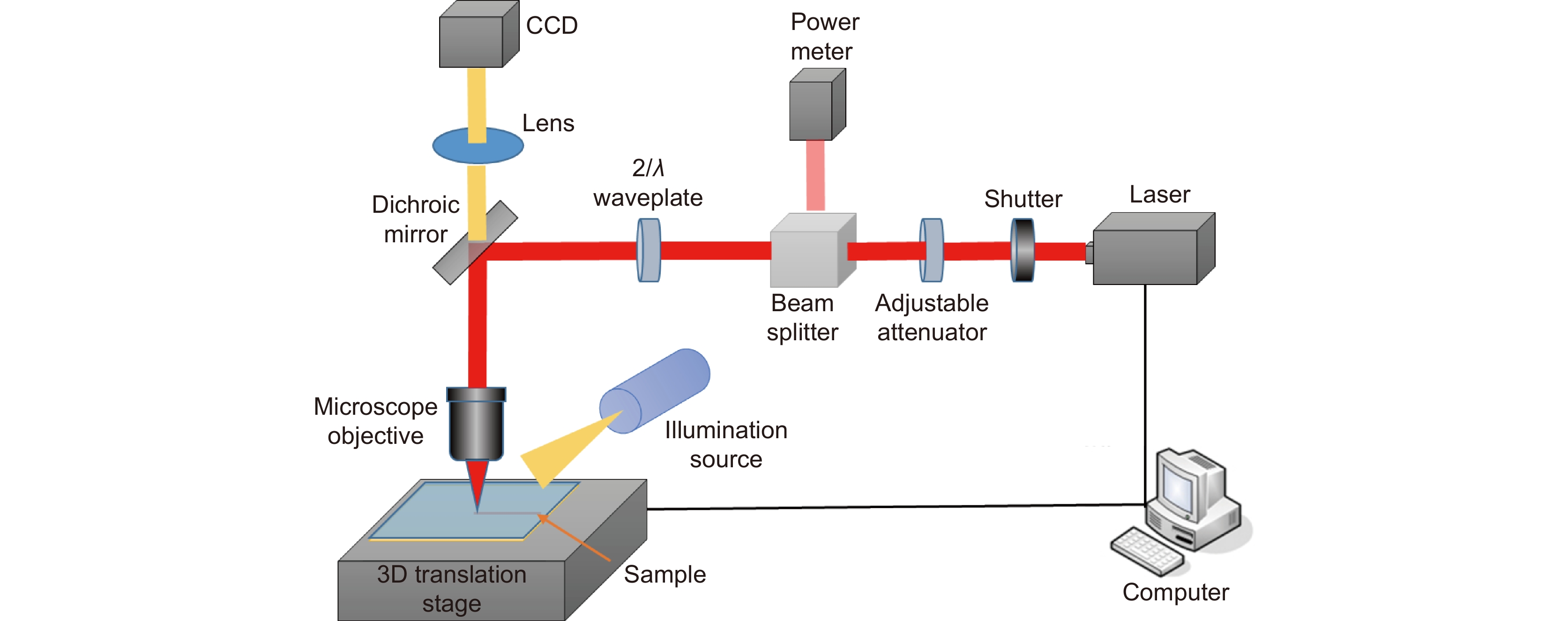
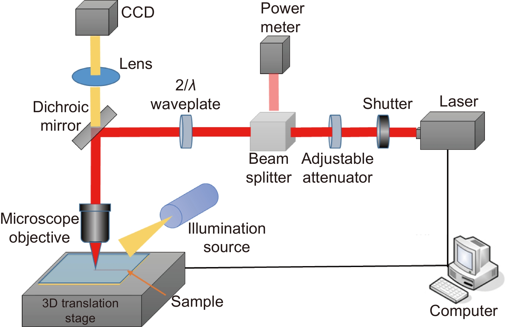
图 1 激光直写加工系统的示意图
Figure 1. Schematic diagram of laser direct writing processing system

图 2 (a) 单光子,(b) 多光子和(c) 热驱动反应类型示意图[19]
Figure 2. Schematic diagram of (a) single photon, (b) multi-photon and (c) thermally driven reaction
-
[1] Ma Z C, Zhang Y L, Han B, et al. Femtosecond-laser direct writing of metallic micro/nanostructures: from fabrication strategies to future applications[J]. Small Methods, 2018, 2(7): 1700413. doi: 10.1002/smtd.201700413
[2] Kim N Y, Adhikari K K, Dhakal R, et al. Rapid, sensitive, and reusable detection of glucose by a robust radiofrequency integrated passive device biosensor chip[J]. Sci Rep, 2015, 5(1): 7807. doi: 10.1038/srep07807
[3] Imboden M, Han H, Chang J, et al. Atomic calligraphy: the direct writing of nanoscale structures using a microelectromechanical system[J]. Nano Lett, 2013, 13(7): 3379−3384. doi: 10.1021/nl401699w
[4] Li Z P, Bao K, Fang Y R, et al. Correlation between incident and emission polarization in nanowire surface plasmon waveguides[J]. Nano Lett, 2010, 10(5): 1831−1835. doi: 10.1021/nl100528c
[5] Zhou W P, Hu A M, Bai S, et al. Anisotropic optical properties of large-scale aligned silver nanowire films via controlled coffee ring effects[J]. RSC Adv, 2015, 5(49): 39103−39109. doi: 10.1039/C5RA04214C
[6] Radha B, Kulkarni G U. An electrical rectifier based on Au nanoparticle array fabricated using direct‐write electron beam lithography[J]. Adv Funct Mater, 2012, 22(13): 2837−2845. doi: 10.1002/adfm.201103170
[7] Zhou W P, Hu A M, Bai S, et al. Surface-enhanced Raman spectra of medicines with large-scale self-assembled silver nanoparticle films based on the modified coffee ring effect[J]. Nanoscale Res Lett, 2014, 9(1): 87. doi: 10.1186/1556-276X-9-87
[8] Lewis J A. Direct ink writing of 3D functional materials[J]. Adv Funct Mater, 2006, 16(17): 2193−2204. doi: 10.1002/adfm.200600434
[9] Zhang C Y, Zhou W, Geng D, et al. Laser direct writing and characterizations of flexible piezoresistive sensors with microstructures[J]. Opto-Electron Adv, 2021, 4(4): 200061.
[10] Maruo S, Nakamura O, Kawata S. Three-dimensional microfabrication with two-photon-absorbed photopolymerization[J]. Opt Lett, 1997, 22(2): 132−134. doi: 10.1364/ol.22.000132
[11] Waller E H, Dix S, Gutsche J, et al. Functional metallic microcomponents via liquid-phase multiphoton direct laser writing: a review[J]. Micromachines, 2019, 10(12): 827. doi: 10.3390/mi10120827
[12] 季春燕, 李新国, 刘恺然, 等. 纳米纸在绿色电子器件中的研究进展[J]. 科技导报, 2019, 37(11): 82−91. doi: 10.3981/j.issn.1000-7857.2019.11.010
Ji C Y, Li X G, Liu K R, et al. Nanocellulose paper fabrication and application in green electronics: a review[J]. Sci Technol Rev, 2019, 37(11): 82−91. doi: 10.3981/j.issn.1000-7857.2019.11.010
[13] Sakaushi K, Antonietti M. Carbon- and nitrogen-based porous solids: a recently emerging class of materials[J]. Bull Chem Soc Jpn, 2015, 88(3): 386−398. doi: 10.1246/bcsj.20140317
[14] Wang H Z, Delacroix S, Osswald O, et al. Laser-carbonization: peering into the formation of micro-thermally produced (N-doped) carbons[J]. Carbon, 2021, 176: 500−510. doi: 10.1016/j.carbon.2021.01.145
[15] Wan Z F, Streed E W, Lobino M, et al. Laser‐reduced graphene: synthesis, properties, and applications[J]. Adv Mater Technol, 2018, 3(4): 1700315. doi: 10.1002/admt.201700315
[16] Huang L B, Su J J, Song Y, et al. Laser-induced graphene: en route to smart sensing[J]. Nano-Micro Lett, 2020, 12(1): 157. doi: 10.1007/s40820-020-00496-0
[17] Niu M C, Yao Y B, Shi Y L, et al. Multifunctional green sensor prepared by direct laser writing of modified wood component[J]. Ind Eng Chem Res, 2019, 58(24): 10364−10372. doi: 10.1021/acs.iecr.9b00850
[18] Arnold C B, Piqué A. Laser direct-write processing[J]. MRS Bull, 2007, 32(1): 9−15. doi: 10.1557/mrs2007.9
[19] Armon N, Greenberg E, Edri E, et al. Laser-based printing: from liquids to microstructures[J]. Adv Funct Mater, 2021, 31(13): 2008547. doi: 10.1002/adfm.202008547
[20] Stampfl J, Baudis S, Heller C, et al. Photopolymers with tunable mechanical properties processed by laser-based high-resolution stereolithography[J]. J Micromechan Microeng, 2008, 18(12): 125014. doi: 10.1088/0960-1317/18/12/125014
[21] Sun C, Fang N, Wu D M, et al. Projection micro-stereolithography using digital micro-mirror dynamic mask[J]. Sens Actuators A Phys, 2005, 121(1): 113−120. doi: 10.1016/j.sna.2004.12.011
[22] Palneedi H, Park J H, Maurya D, et al. Laser irradiation of metal oxide films and nanostructures: applications and advances[J]. Adv Mater, 2018, 30(14): 1705148. doi: 10.1002/adma.201705148
[23] Lachish-Zalait A, Zbaida D, Klein E, et al. Direct surface patterning from solutions: localized microchemistry using a focused laser[J]. Adv Funct Mater, 2001, 11(3): 218−223. doi: 10.1002/1616-3028(200106)11:3<218::AID-ADFM218>3.0.CO;2-T
[24] Tanaka T, Ishikawa A, Kawata S. Two-photon-induced reduction of metal ions for fabricating three-dimensional electrically conductive metallic microstructure[J]. Appl Phys Lett, 2006, 88(8): 081107. doi: 10.1063/1.2177636
[25] Cao Y Y, Takeyasu N, Tanaka T, et al. 3D metallic nanostructure fabrication by surfactant-assisted multiphoton-induced reduction[J]. Small, 2009, 5(10): 1144−1148. doi: 10.1002/smll.200801179
[26] Zhou W P, Bai S, Ma Y, et al. Laser-direct writing of silver metal electrodes on transparent flexible substrates with high-bonding strength[J]. ACS Appl Mater Interfaces, 2016, 8(37): 24887−24892. doi: 10.1021/acsami.6b07696
[27] Zhou W P, Yu Y C, Bai S, et al. Laser direct writing of waterproof sensors inside flexible substrates for wearable electronics[J]. Opt Laser Technol, 2021, 135(11): 106694. doi: 10.1016/j.optlastec.2020.106694
[28] Bai S, Zhang S G, Zhou W P, et al. Laser-assisted reduction of highly conductive circuits based on copper nitrate for flexible printed sensors[J]. Nano-Micro Lett, 2017, 9(4): 49−61. doi: 10.1007/s40820-017-0150-8
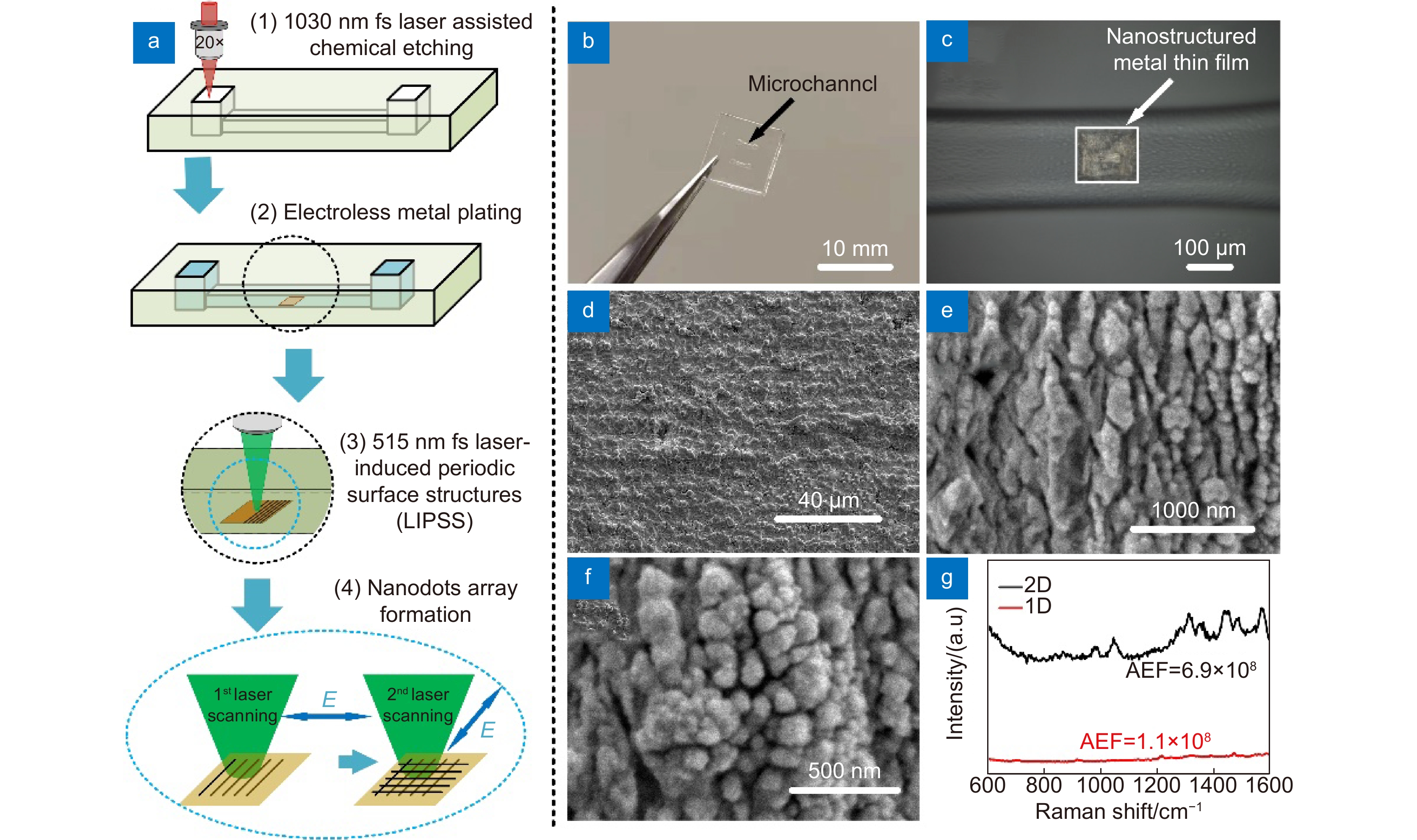
[29] Jo Y, Park H J, Kim Y B, et al. Form‐factor free 3D copper circuits by surface‐conformal direct printing and laser writing[J]. Adv Funct Mater, 2020, 30(45): 2004659. doi: 10.1002/adfm.202004659
[30] Zhou X W, Guo W, Zhu Y, et al. The laser writing of highly conductive and anti-oxidative copper structures in liquid[J]. Nanoscale, 2020, 12(2): 563−571. doi: 10.1039/C9NR07248A
[31] Lu W E, Zhang Y L, Zheng M L, et al. Femtosecond direct laser writing of gold nanostructures by ionic liquid assisted multiphoton photoreduction[J]. Opt Mater Express, 2013, 3(10): 1660−1673. doi: 10.1364/OME.3.001660
[32] Blasco E, Müller J, Müller P, et al. Fabrication of conductive 3D gold‐containing microstructures via direct laser writing[J]. Adv Mater, 2016, 28(18): 3592−3595. doi: 10.1002/adma.201506126
[33] Li R Z, Peng R, Kihm K D, et al. High-rate in-plane micro-supercapacitors scribed onto photo paper using in situ femtolaser-reduced graphene oxide/Au nanoparticle microelectrodes[J]. Energy Environ Sci, 2016, 9(4): 1458−1467. doi: 10.1039/C5EE03637B
[34] Fischer J, Wegener M. Three‐dimensional optical laser lithography beyond the diffraction limit[J]. Laser Photonics Rev, 2013, 7(1): 22−44. doi: 10.1002/lpor.201100046
[35] Kawata S, Sun H B, Tanaka T, et al. Finer features for functional microdevices[J]. Nature, 2001, 412(6848): 697−698. doi: 10.1038/35089130
[36] Bückmann T, Stenger N, Kadic M, et al. Tailored 3D mechanical metamaterials made by dip-in direct-laser-writing optical lithography[J]. Adv Mater, 2012, 24(20): 2710−2714. doi: 10.1002/adma.201200584
[37] Qin L, Huang Y Q, Xia F, et al. 5 nm Nanogap electrodes and arrays by super-resolution laser lithography[J]. Nano Lett, 2020, 20(7): 4916−4923. doi: 10.1021/acs.nanolett.0c00978
[38] Pallaoro A, Hoonejani M R, Braun B B, et al. Rapid identification by surface-enhanced Raman spectroscopy of cancer cells at low concentrations flowing in a microfluidic channel[J]. ACS Nano, 2015, 9(4): 4328−4336. doi: 10.1021/acsnano.5b00750
[39] Wu L, Garrido-Maestu A, Guerreiro J R L, et al. Amplification-free SERS analysis of DNA mutation in cancer cells with single-base sensitivity[J]. Nanoscale, 2019, 11(16): 7781−7789. doi: 10.1039/C9NR00501C
[40] Kim S, Kim T G, Lee S H, et al. Label-free surface-enhanced Raman spectroscopy biosensor for on-site breast cancer detection using human tears[J]. ACS Appl Mater Interfaces, 2020, 12(7): 7897−7904. doi: 10.1021/acsami.9b19421
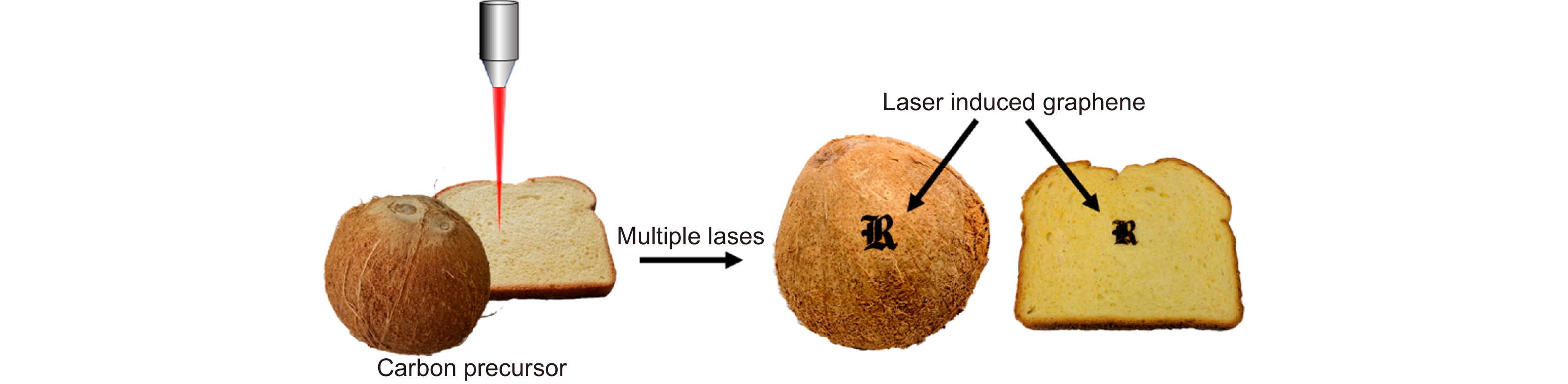
[41] Eom G, Kim H, Hwang A, et al. Nanogap-Rich Au nanowire SERS sensor for ultrasensitive telomerase activity detection: application to gastric and breast cancer tissues diagnosis[J]. Adv Funct Mater, 2017, 27(37): 1701832. doi: 10.1002/adfm.201701832
[42] Liebel M, Pazos-Perez N, van Hulst N F, et al. Surface-enhanced Raman scattering holography[J]. Nat Nanotechnol, 2020, 15(12): 1005−1011. doi: 10.1038/s41565-020-0771-9
[43] Wei J, Qin S N, Liu J L, et al. In situ Raman monitoring and manipulating of interfacial hydrogen spillover by precise fabrication of Au/TiO2/Pt sandwich structures[J]. Angew Chem, 2020, 132(26): 10429−10433. doi: 10.1002/ange.202000426
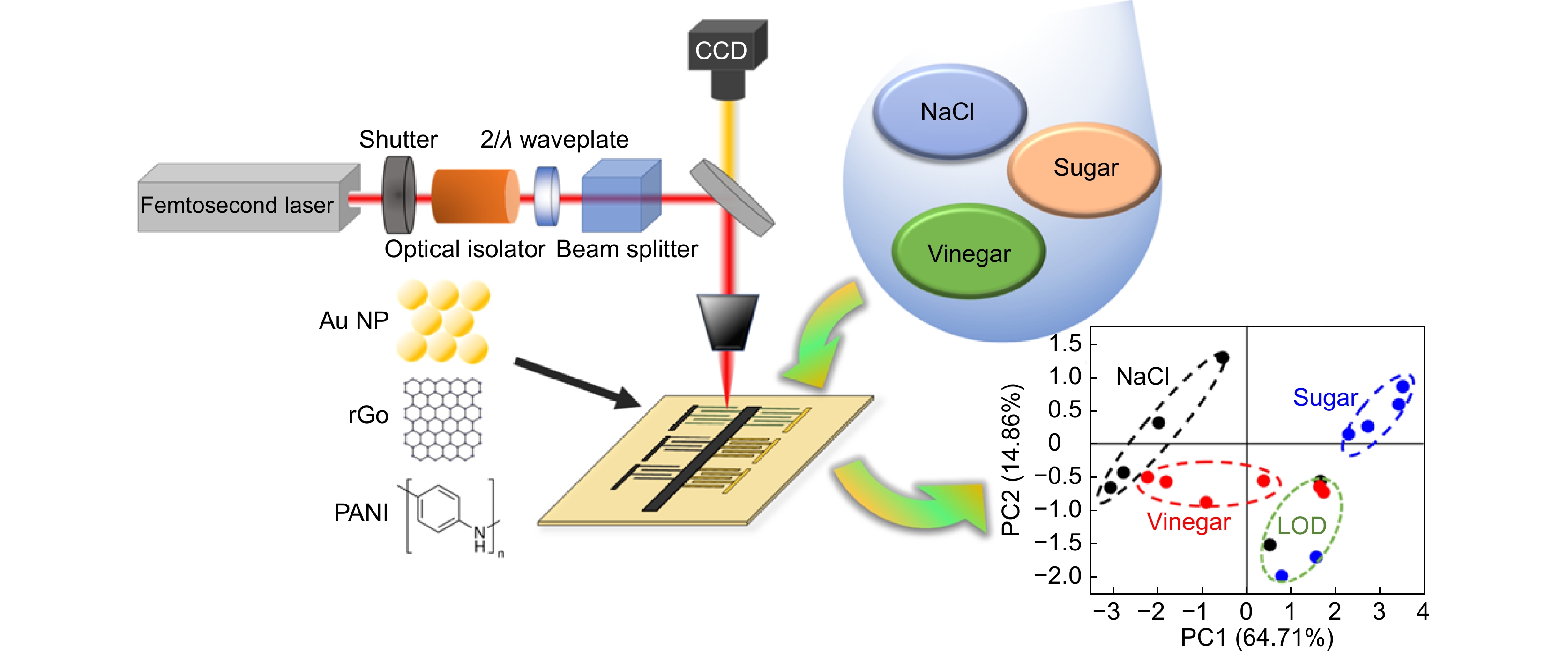
[44] Jeong H, Jongwon K. Insights into the electrooxidation mechanism of formic acid on Pt layers on Au examined by electrochemical SERS[J]. J Phys Chem C, 2016, 120(42): 24271−24278. doi: 10.1021/acs.jpcc.6b08611
[45] Shan W Y, Liu R, Zhao H C, et al. In situ surface-enhanced Raman spectroscopic evidence on the origin of selectivity in CO2 electrocatalytic reduction[J]. ACS Nano, 2020, 14(9): 11363−11372. doi: 10.1021/acsnano.0c03534
[46] Bai S, Serien D, Hu A M, et al. 3D microfluidic surface-Enhanced Raman Spectroscopy (SERS) chips fabricated by all-femtosecond-laser-processing for real-time sensing of toxic substances[J]. Adv Funct Mater, 2018, 28(23): 1706262. doi: 10.1002/adfm.201706262
[47] Bai S, Serien D, Ma Y, et al. Attomolar sensing based on liquid interface-assisted surface-enhanced Raman scattering in microfluidic chip by femtosecond laser processing[J]. ACS Appl Mater Interfaces, 2020, 12(37): 42328−42338. doi: 10.1021/acsami.0c11322
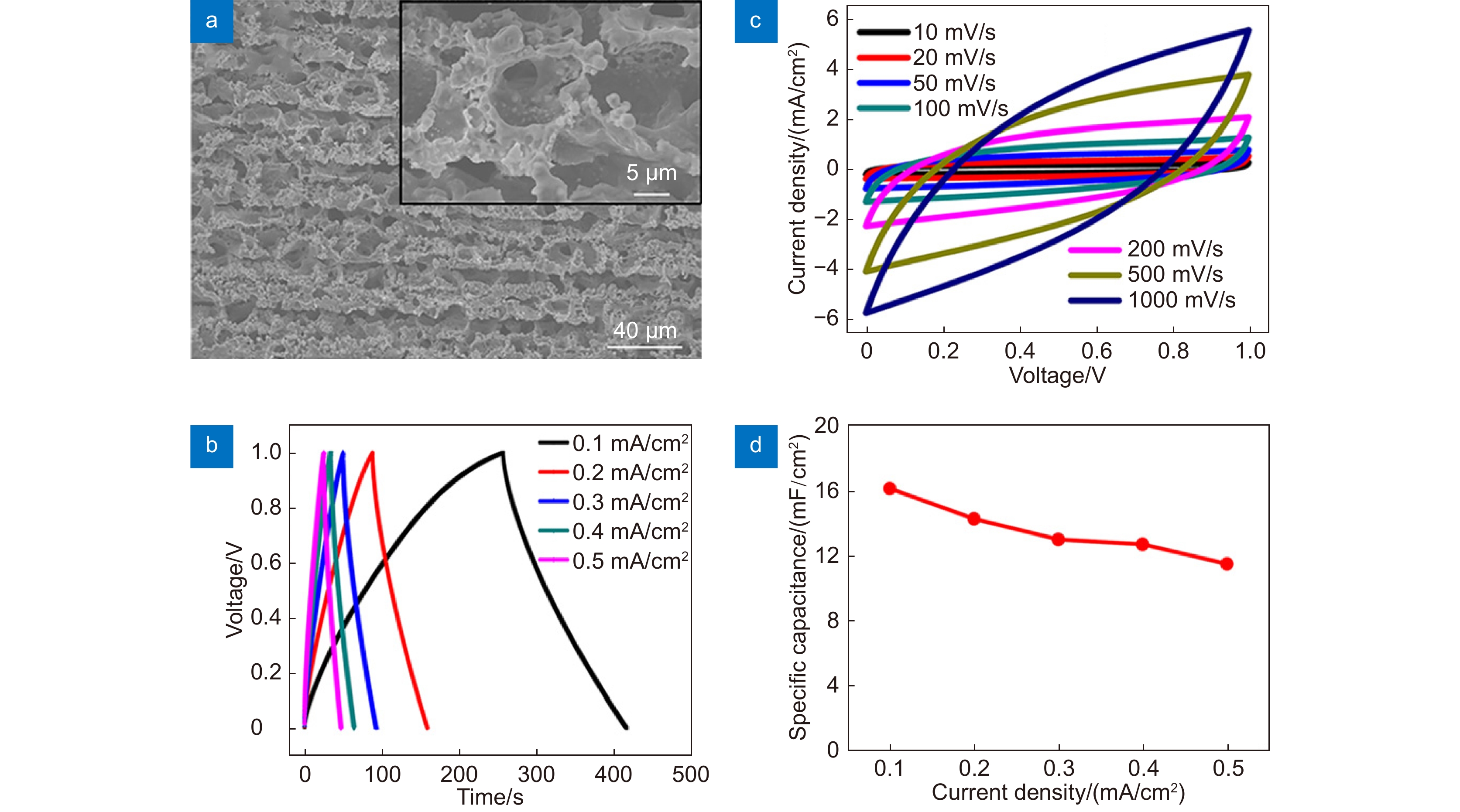
[48] Yoshikawa H, Hironou A, Shen Z J, et al. Versatile micropatterning of plasmonic nanostructures by visible light induced electroless silver plating on gold nanoseeds[J]. ACS Appl Mater Interfaces, 2016, 8(36): 23932−23940. doi: 10.1021/acsami.6b07661
[49] Xu B B, Ma Z C, Wang L, et al. Localized flexible integration of high-efficiency surface enhanced Raman scattering (SERS) monitors into microfluidic channels[J]. Lab Chip, 2011, 11(19): 3347−3351. doi: 10.1039/c1lc20397e
[50] MacKenzie M, Chi H N, Varma M, et al. Femtosecond laser fabrication of silver nanostructures on glass for surface enhanced Raman spectroscopy[J]. Sci Rep, 2019, 9(1): 17058. doi: 10.1038/s41598-019-53328-6
[51] Izquierdo-Lorenzo I, Jradi S, Adam P M. Direct laser writing of random Au nanoparticle three-dimensional structures for highly reproducible micro-SERS measurements[J]. RSC Adv, 2014, 4(8): 4128−4133. doi: 10.1039/C3RA46220J
[52] Ran P, Jiang L, Li X, et al. Femtosecond Photon-mediated plasma enhances photosynthesis of plasmonic nanostructures and their SERS applications[J]. Small, 2019, 15(11): 1804899. doi: 10.1002/smll.201804899
[53] Lin Z Y, Liu H G, Ji L F, et al. Realization of ∼10 nm features on semiconductor surfaces via femtosecond laser direct patterning in far field and in ambient air[J]. Nano Lett, 2020, 20(7): 4947−4952. doi: 10.1021/acs.nanolett.0c01013
[54] Plech A, Leiderer P, Boneberg J. Femtosecond laser near field ablation[J]. Laser Photonics Rev, 2009, 3(5): 435−451. doi: 10.1002/lpor.200810044
[55] Feng D, Weng D, Wang B, et al. Laser pulse number dependent nanostructure evolution by illuminating self-assembled microsphere array[J]. J Appl Phys, 2017, 122(24): 243102. doi: 10.1063/1.5000275
[56] Le T S D, Park S, An J N, et al. Ultrafast laser pulses enable one‐step graphene patterning on woods and leaves for green electronics[J]. Adv Funct Mater, 2019, 29(33): 1902771. doi: 10.1002/adfm.201902771
[57] Ye R Q, Chyan Y, Zhang J B, et al. Laser‐induced graphene formation on wood[J]. Adv Mater, 2017, 29(37): 1702211. doi: 10.1002/adma.201702211
[58] Chyan Y, Ye R Q, Li Y L, et al. Laser-induced graphene by multiple lasing: toward electronics on cloth, paper, and food[J]. ACS Nano, 2018, 12(3): 2176−2183. doi: 10.1021/acsnano.7b08539
[59] Lei Y J, Alshareef A H, Zhao W L, et al. Laser-scribed graphene electrodes derived from lignin for biochemical sensing[J]. ACS Appl Nano Mater, 2020, 3(2): 1166−1174. doi: 10.1021/acsanm.9b01795
[60] Morosawa F, Hayashi S, Terakawa M. Femtosecond laser-induced graphitization of transparent cellulose nanofiber films[J]. ACS Sustainable Chem Eng, 2021, 9(7): 2955−2961. doi: 10.1021/acssuschemeng.0c09153
[61] Yu Y C, Joshi P C, Wu J, et al. Laser-induced carbon-based smart flexible sensor array for multiflavors detection[J]. ACS Appl Mater Interfaces, 2018, 10(40): 34005−34012. doi: 10.1021/acsami.8b12626
[62] Kim Y J, Le T S D, Nam H K, et al. Wood-based flexible graphene thermistor with an ultra-high sensitivity enabled by ultraviolet femtosecond laser pulses[J]. CIRP Ann, 2021, 70(1): 443−446. doi: 10.1016/j.cirp.2021.04.031
[63] Ji X J, Zhong Y, Li C Y, et al. Nanoporous carbon aerogels for laser-printed wearable sensors[J]. ACS Appl Nano Mater, 2021, 4(7): 6796−6804. doi: 10.1021/acsanm.1c00858
[64] Wan Z F, Chen X, Gu M. Laser scribed graphene for supercapacitors[J]. Opto-Electron Adv, 2021, 4(7): 200079. doi: 10.29026/oea.2021.200079
[65] Wang S T, Yu Y C, Luo S, et al. All-solid-state supercapacitors from natural lignin-based composite film by laser direct writing[J]. Appl Phys Lett, 2019, 115(8): 083904. doi: 10.1063/1.5118340
[66] Wang S T, Yu Y C, Li R Z, et al. High-performance stacked in-plane supercapacitors and supercapacitor array fabricated by femtosecond laser 3D direct writing on polyimide sheets[J]. Electrochim Acta, 2017, 241: 153−161. doi: 10.1016/j.electacta.2017.04.138
-
 下载:
下载:
 点击扫一扫
点击扫一扫
图(10)
计量
- 文章访问数:
- PDF下载数:
- 施引文献: 0


