
 E-mail Alert
 RSS
RSS
Transmission characteristics of a Y-shaped MIM plasmonic waveguide with side-coupled cavities
-
摘要
本文设计了一种带有两个水平侧耦合Fabry-Perot (FP)共振腔的基于金属-绝缘体-金属(MIM)结构的Y型表面等离子体光波导结构。传输谱存在一个较窄的阻带,两个腔的长度相同时,两个输出端的传输谱几乎完全重合;两个腔长度不同时每个输出端的传输谱上的阻带位置也不同,并且当一个输出端透射率达到最小时,另一个输出端的透射率接近最大。通过调节两个FP共振腔的长度、宽度以及腔内介质的折射率,可以调节表面等离子体激元在腔内发生共振从而形成驻波的工作波长,实现探测灵敏度高达1280 nm/RIU、品质因子大于200的传感特性。利用这些特性可以在两个输出端对不同的工作波长实现滤波、开关、分束等功能,因此这种亚波长表面等离子体光波导结构在集成光学滤波器、纳米光开关、分束器以及折射率传感器等领域有一定的应用前景。

Abstract
A plasmonic Y-shaped metal-insulator-metal (MIM) plasmonic waveguide with two side-coupled Fabry–Perot (FP) resonant cavities is proposed. Simulation results show that there is a stopband existing in the transmission spectrum of each output port. When the lengths of the two cavities are equal, the transmission spectra of the two output ports are almost coincident. But if they are not equal, the two stopbands are not in the same place. Meanwhile, the transmission dip of one output port corresponds to the transmission peak of another port. By adjusting the length, width and refractive index of the two FP cavities, one can control the resonant wavelength of each cavity to further achieve functions of filtering, power splitting, switching and refractive index sensing. Results show that the sensing sensitivity is up to 1280 nm/RIU with its figure of merit above 200 when the waveguide is used as a refractive sensor. The proposed waveguide structure has potential applications in the fields of integrated optical filter, nano-optic switch, power splitter and refractive sensor in subwavelength scale.
-
Key words:
- surface plasmonic waveguide /
- transmission spectrum /
- resonance
-
Overview

Surface plasmon polaritons (SPPs) is a type of collective electron oscillation along metal-dielectric interface. Based on the coupling between the incident light and the free electrons metal surface, it can propagate along the interface with an exponentially decaying field distribution on both sides. SPPs may be one of the most promising candidates in the area of nano integrated optics because of the subwavelength optical confinement with the ability of breaking the diffraction limit. During the past years, advancements in novel plasmon waveguide configurations have led to the proposal and demonstration of numerous plasmon waveguide structures, which combine the advantages of both semiconductor and plasmon waveguides and enable light transmission in the deep sub-wavelength scale to achieve long distance propagating with very tight mode confinement. Among these waveguides, the metal-insulator-metal (MIM) waveguides have attracted considerable interests because of their smaller mode size, stronger confinement of SPPs and lower propagation loss. They are promising structures for design of nanoscale all-optical devices due to their relatively easy fabrication according to the current state of the art. Optical resonant cavities based on the MIM structures are crucial structural components in plasmonic wavelength-selective devices and plasmonic all-optical switches owing to their simplicity. A plasmonic Y-shaped metal-insulator-metal (MIM) plasmonic waveguide structure with two side-coupled Fabry–Perot (FP) resonant cavities is proposed. The finite element method (FEM) is used to study the transmission properties of the waveguide. Simulation results show that two stopbands occur respectively on the transmission spectrum of each output port and which is helpful to the potential applications of narrowband filter. In addition, at other locations in the spectra away from the stopbands, the transmission rates of the two output ports are always equal indicating obvious effect of optical splitting. By tuning the lengths of the two cavities, the locations of the stopbands can be effectively controlled, and an interesting phenomenon is that the transmission peak of one output port corresponds to the transmission dip of another output port. Based on this result, the effect of all-optical directional transmission, switching and filtering can be obtained and adjusted by changing the geometry parameters. Finally, the applications of the structure in the area of refractive index sensing are investigated. For this purpose, the sample to be measured can be filled in two the cavities. During the simulation, the refractive index of the medium filled in the cavities is changed from 1.00 to 1.05 with a step of 0.01. It is found that the transmission spectra of the two output ports have a clear redshift, and the calculated sensitivity can reach 1280 nm/RIU with the quality factor up to 208. The proposed compact waveguide structure has potential applications in the field of integrated photonic devices, such as plasmonic filters, switches, power splitters and refractive sensors.
-

-
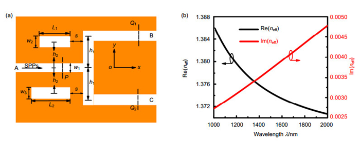
图 1 (a) 结构原理图. (b)介质层宽度50 nm时MIM结构有效折射率的实部和虚部与波长的关系.
Figure 1. (a) Schematic plot of the designed structure. (b) Real and imaginary part of the effective mode index as a function of the wavelength when the thickness of insulator layer is 50 nm.

图 2 侧耦合腔左右两侧的反射率和透射率随(a)入射光波长和(b)耦合间隔s的变化关系.其中,w=50 nm, 且图(a)中s=10 nm,图(b)中波长为1550 nm.
Figure 2. Reflection and transmission of the left and right sides of the side-coupled cavity as a function of (a) incident wavelength, (b) coupling distance s when w=50 nm, with s=10 nm in (a) and wavelength of 1550 nm in (b).

图 3 两个输出端的传输谱. (a) L1=L2=L=420 nm. (b) L1=L2=L=510 nm. (c)和(d)分别是波长为1303 nm和1546 nm时的磁场分量|Hz|的分布图.其中,s=10 nm, h1=170 nm, h2=120 nm.
Figure 3. Transmission spectra of the two output ports. (a) L1=L2=L=420 nm. (b) L1=L2=L=510 nm. (c), (d) are the distributions of |Hz| at the wavelength of 1303 nm and 1546 nm. Here, s=10 nm, h1=170 nm, h2=120 nm.
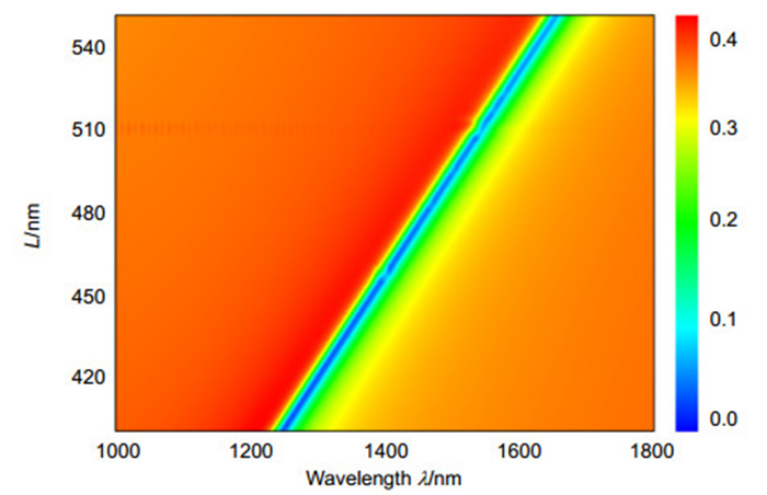
图 4 L1=L2=L, w=50 nm, s=10 nm, h1=170 nm, h2=120 nm时的透射率伪色图.
Figure 4. Pseudo color map of the transmission spectra when L1=L2=L, w=50 nm, s=10 nm, h1=170 nm, h2=120 nm.
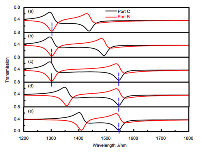
图 5 两个输出端的传输谱. (a) L1=420 nm, L2=470 nm. (b) L1=420 nm, L2=490 nm. (c) L1=420 nm, L2=510 nm. (d) L1=440 nm, L2=510 nm. (e) L1=460 nm, L2=510 nm.
Figure 5. Transmission spectra of the two output ports. (a) L1=420 nm, L2=470 nm. (b) L1=420 nm, L2=490 nm. (c) L1=420 nm, L2=510 nm. (d) L1=440 nm, L2=510 nm. (e) L1=460 nm, L2=510 nm.
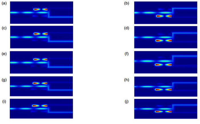
图 6 传输谷值波长处的磁场分布. (a)和(b)、(c)和(d)、(e)和(f)、(g)和(h)、(i)和(j)分别对应图 5(a)、5(b)、5(c)、5(d)和5(e).
Figure 6. Magnetic field distributions of |Hz| at the transmission dips. (a) and (b), (c) and (d), (e) and (f), (g) and (h), (i) and (j) correspond to the two transmission dips of Figs. 5(a), 5(b), 5(c), 5(d) and 5(e) respectively.
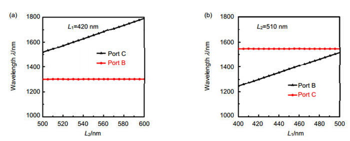
图 7 端口B和端口C透射率谷值波长变化. (a) L1=420 nm, L2以步长5 nm从500 nm增加到600 nm. (b) L2=510 nm, L1以步长5 nm从400 nm增加到500 nm.
Figure 7. Variation of dip wavelength in transmission spectra for Port B and Port C. (a) L1=420 nm, L2 increases from 500 nm to 600 nm with a step of 5 nm. (b) L2=510 nm, L1 increases from 400 nm to 500 nm with a step of 5 nm.

图 8 (a) L1=420 nm, L2=510 nm. (b) L1=430 nm, L2=500 nm, and (c) L1=440 nm, L2=490 nm时的传输谱.
Figure 8. Transmission spectra with (a) L1=420 nm, L2=510 nm. (b) L1=430 nm, L2=500 nm, and (c) L1=440 nm, L2=490 nm.

图 9 两个FP腔长同时增加时的传输谱. (a) L1=400 nm, L2=490 nm. (b) L1=410 nm, L2=500 nm. (c) L1=420 nm, L2=510 nm. (d) L1=430 nm, L2=520 nm and (e) L1=440 nm, L2=530 nm.
Figure 9. Transmission spectra when the lengths of two FP cavities increase simultaneously. (a) L1=400 nm, L2=490 nm. (b) L1=410 nm, L2=500 nm. (c) L1=420 nm, L2=510 nm. (d) L1=430 nm, L2=520 nm and (e) L1=440 nm, L2=530 nm.
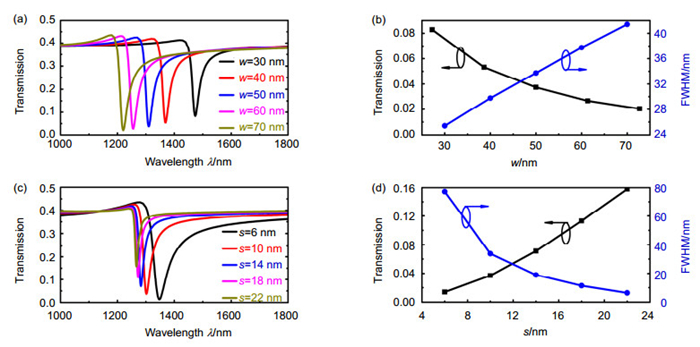
图 10 (a) 共振腔宽度不同的传输谱. (b)共振腔宽度增加时谷值传输率和半高全宽的变化. (c)耦合距离不同的传输谱. (d)耦合距离增加时谷值传输率和半高全宽的变化.这里L1=L2=420 nm, s=10 nm, h1=170 nm, h2=120 nm, w=50 nm.
Figure 10. Transmission spectra of (a) different resonator width, (c) different coupling distance. Transmission dip wavelength and FWHM as a function of (b) resonator width w, and (d) coupling distance s. Here, L1=L2=420 nm, s=10 nm, h1=170 nm, h2=120 nm, and w=50 nm.
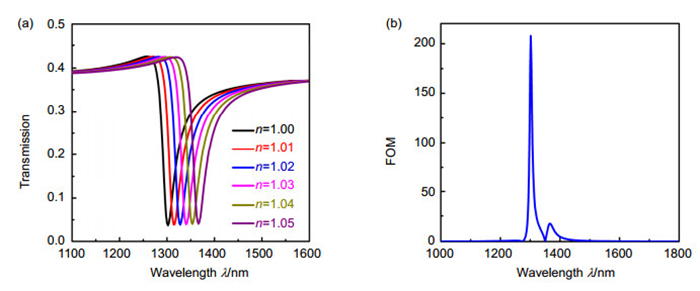
图 11 (a) 腔内待测样品折射率取不同值时的传输谱曲线. (b)品质因数演化曲线.这里L1=L2=420 nm, h1=170 nm, h2=120 nm.
Figure 11. (a) Transmission spectra for different refractive index of the sample to be detected in the resonator and (b) the calculated FOM as a function of working wavelength. Here, L1=L2=420 nm, h1=170 nm, h2=120 nm.
表 1 耦合距离s和侧耦合腔宽度w取不同值时的谷值波长以及求得的品质因子Qt, Q0和Qe.
Table 1. The dip wavelength and calculated quality factors of Qt, Q0 and Qe for different coupling distance s and different cavity width w.
s/nm λ Qt Q0 Qe w/nm λ Qt Q0 Qe 6 1348 18 202 20 30 1474 58 188 84 10 1303 39 208 48 40 1370 46 200 60 14 1283 68 211 100 50 1303 39 208 48 18 1273 111 212 233 60 1256 33 214 39 22 1267 198 213 2812 70 1220 30 220 35  下载: 导出CSV
-
参考文献
[1] Barnes W L, Dereux A, Ebbesen T W. Surface plasmon subwavelength optics[J]. Nature, 2003, 424(6950): 824-830. doi: 10.1038/nature01937 http://cn.bing.com/academic/profile?id=b4b6774ed503181556d498ff2abee3d3&encoded=0&v=paper_preview&mkt=zh-cn
[2] 林佼, 王大鹏, 司光远.表面等离子激元超构表面的研究进展[J].光电工程, 2017, 44(3): 289-296. http://www.oejournal.org/J/OEE/Article/Details/A170427000020/CN
Lin Jiao, Wang Dapeng, Si Guangyuan. Recent progress on plasmonic metasurfaces[J]. Opto-Electronic Engineering, 2017, 44(3): 289-296. http://www.oejournal.org/J/OEE/Article/Details/A170427000020/CN
[3] Bian Yusheng, Gong Qihuang. Low-loss hybrid plasmonic modes guided by metal-coated dielectric wedges for subwavelength light confinement[J]. Applied Optics, 2013, 52(23): 5733-5741. doi: 10.1364/AO.52.005733 http://cn.bing.com/academic/profile?id=598fdf17e3297221059e35ad26eefb7f&encoded=0&v=paper_preview&mkt=zh-cn
[4] Dai Daoxin, He Sailing. A silicon-based hybrid plasmonic waveguide with a metal cap for a nano-scale light confinement[J]. Optics Express, 2009, 17(19): 16646-16653. doi: 10.1364/OE.17.016646 http://cn.bing.com/academic/profile?id=d512b7e7ef7d7423494476591a671e97&encoded=0&v=paper_preview&mkt=zh-cn
[5] Taubert R, Hentschel M, Giessen H. Plasmonic analog of electromagnetically induced absorption: Simulations, experiments, and coupled oscillator analysis[J]. Journal of the Optical Society of America B, 2013, 30(12): 3123-3134. doi: 10.1364/JOSAB.30.003123 http://cn.bing.com/academic/profile?id=d313d7dc41d21864051b3d07a41261eb&encoded=0&v=paper_preview&mkt=zh-cn
[6] Han Zhanghua, Bozhevolnyi S I. Radiation guiding with surface plasmon polaritons[J]. Reports on Progress in Physics, 2013, 76(1): 016402. doi: 10.1088/0034-4885/76/1/016402 http://cn.bing.com/academic/profile?id=0cd4cff0d2432a0e256a13f4716bf22f&encoded=0&v=paper_preview&mkt=zh-cn
[7] 方佳文, 张明, 张飞, 等.基于Fano共振的等离子体共振传感器[J].光电工程, 2017, 44(2): 221-225. http://www.oejournal.org/J/OEE/Article/Details/A170317000599/CN
Fang Jiawen, Zhang Ming, Zhang Fei, et al. Plasmonic sensor based on Fano resonance[J]. Opto-Electronic Engineering, 2017, 44(2): 221-225. http://www.oejournal.org/J/OEE/Article/Details/A170317000599/CN
[8] Pu Mingbo, Ma Xiaoliang, Li Xiong, et al. Merging plasmonics and metamaterials by two-dimensional subwavelength structures[J]. Journal of Materials Chemistry C, 2017, 5(18): 4361-4378. doi: 10.1039/C7TC00440K http://pubs.rsc.org/en/content/articlelanding/2017/tc/c7tc00440k#!
[9] Nikolajsen T, Leosson K. Surface plasmon polariton based modulators and switches operating at telecom wavelengths[J]. Applied Physics Letters, 2004, 85(24): 5833-5835. doi: 10.1063/1.1835997 http://cn.bing.com/academic/profile?id=63f85367c9c640772fb50194d3ea1ded&encoded=0&v=paper_preview&mkt=zh-cn
[10] Liu Jianqiang, Wang Lingling, He Mengdong, et al. A wide bandgap plasmonic Bragg reflector[J]. Optics Express, 2008, 16(7): 4888-4894. doi: 10.1364/OE.16.004888 http://cn.bing.com/academic/profile?id=912f21aa821b7f0063a7505ed7330816&encoded=0&v=paper_preview&mkt=zh-cn
[11] Tao Jin, Wang Qijie, Huang Xuguang. All-optical plasmonic switches based on coupled nano-disk cavity structures containing nonlinear material[J]. Plasmonics, 2011, 6(4): 753-759. doi: 10.1007/s11468-011-9260-1 http://www.ntu.edu.sg/home/qjwang/publication/2011_45_Jin%20Tao_Plasmonics.pdf
[12] Veronis G, Fan Shanhui. Bends and splitters in metal-dielectric-metal subwavelength plasmonic waveguide[J]. Applied Physics Letters, 2005, 87(13): 131102. doi: 10.1063/1.2056594 http://cn.bing.com/academic/profile?id=8873a134babbac397a1b37751d3f497a&encoded=0&v=paper_preview&mkt=zh-cn
[13] Gao Hongtao, Shi Haofei, Wang Changtao, et al. Surface plasmon polariton propagation and combination in Y-shaped metallic channels[J]. Optics Express, 2005, 13(26): 10795-10800. doi: 10.1364/OPEX.13.010795 http://cn.bing.com/academic/profile?id=94e3a33031de8d61367b0e04678dfafa&encoded=0&v=paper_preview&mkt=zh-cn
[14] Hosseini A, Massoud Y. Nanoscale surface plasmon based resonator using rectangular geometry[J]. Applied Physics Letters, 2007, 90(18): 181102. doi: 10.1063/1.2734380
[15] 吴德昌, 杨树.等离子体诱导透明的T形-圆形波导滤波器[J].发光学报, 2016, 37(10): 1287-1291. http://kns.cnki.net/KCMS/detail/detail.aspx?filename=fgxb201610019&dbname=CJFD&dbcode=CJFQ
Wu Dechang, Yang Shu. Double-sided T-shaped-disk waveguide filters based on plasmon-induced transparency[J]. Chinese Journal of Luminescence, 2016, 37(10): 1287-1291. http://kns.cnki.net/KCMS/detail/detail.aspx?filename=fgxb201610019&dbname=CJFD&dbcode=CJFQ
[16] Tao Jin, Huang Xuguang, Lin Xianshi, et al. A narrow-band subwavelength plasmonic waveguide filter with asymmetrical multiple-teeth-shaped structure[J]. Optics Express, 2009, 17(16): 13989-13994. doi: 10.1364/OE.17.013989 http://cn.bing.com/academic/profile?id=9406eb5ef818ef21290de4106ac28b8b&encoded=0&v=paper_preview&mkt=zh-cn
[17] Tao Jin, Huang Xuguang, Zhu Jiahu. A wavelength demultiplexing structure based on metal-dielectric-metal plasmonic nano-capillary resonators[J]. Optics Express, 2010, 18(11): 11111-11116. doi: 10.1364/OE.18.011111 http://cn.bing.com/academic/profile?id=6e70bf7dfba437e88e44fc1030973f81&encoded=0&v=paper_preview&mkt=zh-cn
[18] Zhu Jiahu, Huang Xuguang, Tao Jin, et al. A nanometeric plasmonic wavelength demultiplexer based on a T-shaped waveguide structure with double teeth-shaped waveguide at telecommunication wavelengths[J]. Journal of Modern Optics, 2010, 57(21): 2154-2158. doi: 10.1080/09500340.2010.529950 http://cn.bing.com/academic/profile?id=50da7a5bdb122332126b38804bf89ce2&encoded=0&v=paper_preview&mkt=zh-cn
[19] Hu Feifei, Yi Huaxiang, Zhou Zhiping. Wavelength demultiplexing structure based on arrayed plasmonic slot cavities[J]. Optics Letters, 2011, 36(8): 1500-1502. doi: 10.1364/OL.36.001500 http://cn.bing.com/academic/profile?id=69e4e92d4069f36881e8f3ed263d5022&encoded=0&v=paper_preview&mkt=zh-cn
[20] Lu Hua, Liu Xueming, Gong Yongkang, et al. Enhancement of transmission efficiency of nanoplasmonic wavelength demultiplexer based on channel drop filters and reflection nanocavities[J]. Optics Express, 2011, 19(14): 12885-12890. doi: 10.1364/OE.19.012885 http://cn.bing.com/academic/profile?id=bc1804ffefbf191d7ad36d5db6a2ef61&encoded=0&v=paper_preview&mkt=zh-cn
[21] Wang Tongbiao, Wen Xiewen, Yin Chengping, et al. The transmission characteristics of surface plasmon polaritons in ring resonator[J]. Optics Express, 2009, 17(26): 24096-24101. doi: 10.1364/OE.17.024096 http://cn.bing.com/academic/profile?id=306a895e62e2da9eb4e344eb8578468a&encoded=0&v=paper_preview&mkt=zh-cn
[22] Yun Binfeng, Hu Guohua, Cui Yiping. Theoretical analysis of a nanoscale plasmonic filter based on a rectangular metal-insulator-metal waveguide[J]. Journal of Physics D: Applied Physics, 2010, 43(38): 385102. doi: 10.1088/0022-3727/43/38/385102 http://cn.bing.com/academic/profile?id=97b337eda290fabf3e9043ec0ba96b39&encoded=0&v=paper_preview&mkt=zh-cn
[23] Setayesh A, Mirnaziry S R, Abrishamian M S. Numerical investigation of a tunable band-pass plasmonic filter with a hollow-core ring resonator[J]. Journal of Optics, 2011, 13(3): 035004. doi: 10.1088/2040-8978/13/3/035004 http://cn.bing.com/academic/profile?id=3e64f99bd7bebe4e536fb54a17b43c9b&encoded=0&v=paper_preview&mkt=zh-cn
[24] Lin Xianshi, Huang Xuguang. Tooth-shaped plasmonic waveguide filters with nanometeric sizes[J]. Optics Letters, 2008, 33(23): 2874-2876. doi: 10.1364/OL.33.002874 http://cn.bing.com/academic/profile?id=7915fbab928501f3088782fc2b76923f&encoded=0&v=paper_preview&mkt=zh-cn
[25] Hwang Y, Kim J E, Park H Y. Frequency selective metal-insulator-metal splitters for surface plasmons[J]. Optics Communications, 2011, 284(19): 4778-4781. doi: 10.1016/j.optcom.2011.05.069 http://cn.bing.com/academic/profile?id=e1f239b568d2756411cb42d5147d736a&encoded=0&v=paper_preview&mkt=zh-cn
[26] 李娟, 王冰艳, 薛文瑞.基于MIM型表面等离子体光波导的Y形分束器的传输特性研究[J].光学学报, 2012, 32(1): 0124002. http://kns.cnki.net/KCMS/detail/detail.aspx?filename=gxxb201201042&dbname=CJFD&dbcode=CJFQ
Li Juan, Wang Bingyan, Xue Wenrui. Propagation properties of Y-splitters based on MIM surface plasmonic waveguides[J]. Acta Optica Sinica, 2012, 32(1): 0124002. http://kns.cnki.net/KCMS/detail/detail.aspx?filename=gxxb201201042&dbname=CJFD&dbcode=CJFQ
[27] Wen Kunhua, Hu Yihua, Chen Li, et al. Plasmonic bidirectional/unidirectional wavelength splitter based on metal-dielectric-metal waveguides[J]. Plasmonics, 2016, 11(1): 71-77. doi: 10.1007/s11468-015-0021-4 https://rd.springer.com/content/pdf/10.1007%2Fs11468-015-0021-4.pdf
[28] Veronis G, Fan Shihui. Bends and splitters in metal-dielectric-metal subwavelength plasmonic waveguides[J]. Applied Physics Letters, 2005, 87(13): 131102. doi: 10.1063/1.2056594 http://cn.bing.com/academic/profile?id=8873a134babbac397a1b37751d3f497a&encoded=0&v=paper_preview&mkt=zh-cn
[29] 秦小娟, 郭亚楠, 薛文瑞.双正方形中空表面等离子体光波导的传输特性研究[J].光学学报, 2010, 30(12): 3537-3541. http://kns.cnki.net/KCMS/detail/detail.aspx?filename=gxxb201012033&dbname=CJFD&dbcode=CJFQ
Qin Xiaojuan, Guo Ya'nan, Xue Wenrui. Propagation properties of a surface-plasmonic waveguide with a double-square-shaped air core[J]. Acta Optica Sinica, 2010, 30(12): 3537-3541. http://kns.cnki.net/KCMS/detail/detail.aspx?filename=gxxb201012033&dbname=CJFD&dbcode=CJFQ
[30] Li Qiang, Wang Tao, Su Yikai, et al. Coupled mode theory analysis of mode-splitting in coupled cavity system[J]. Optics Express, 2010, 18(8): 8367-8382. doi: 10.1364/OE.18.008367 http://cn.bing.com/academic/profile?id=b4645f219406c1724d27b4a9966512d0&encoded=0&v=paper_preview&mkt=zh-cn
[31] 蒋永翔, 刘炳红, 朱晓松, 等.镀银空芯光纤表面等离子体共振传感器的研究[J].光学学报, 2014, 34(2): 0223004. http://kns.cnki.net/KCMS/detail/detail.aspx?filename=gxxb201402040&dbname=CJFD&dbcode=CJFQ
Jiang Yongxiang, Liu Binghong, Zhu Xiaosong, et al. Study of silver coated hollow-core fiber surface plasmon resonance sensor[J]. Acta Optica Sinica, 2014, 34(2): 0223004. http://kns.cnki.net/KCMS/detail/detail.aspx?filename=gxxb201402040&dbname=CJFD&dbcode=CJFQ
[32] Chen Jianjun, Li Zhi, Zou Yujiao, et al. Coupled-resonator-induced Fano resonances for plasmonic sensing with ultra-high figure of merits[J]. Plasmonics, 2013, 8(4): 1627-1631. doi: 10.1007/s11468-013-9580-4 https://rd.springer.com/content/pdf/10.1007%2Fs11468-013-9580-4.pdf
[33] Wen Kunhua, Hu Yihua, Chen Li, et al. Subwavelength filter and sensor design based on end-coupled composited ring-groove resonator[J]. Opto-Electronic Engineering, 2017, 44(2): 192-197.
-
访问统计
 点击扫一扫
点击扫一扫
图(11)
表(1)
计量
- 文章访问数:
- PDF下载数:
- 施引文献: 0


