
 E-mail Alert
 RSS
RSS
-
摘要
本文报道了一种基于黑硅微结构的全硅PIN光电探测器。该器件结合了黑硅结构宽光谱高吸收的特性,以及PIN光电探测器高量子效率高响应速度的特点,通过在传统硅PIN光电探测器结构的基础上增加黑硅微结构层,在不影响响应速度的条件下,提高了探测器在近红外波段响应特性。并且针对纵向结构垂直入射PIN光电探测器时量子效率与响应速度相矛盾的问题,提出了解决方案。测试结果表明,该器件的量子效率可达80%,峰值波长为940 nm,光响应度达到0.55 A/W,暗电流降至700 pA,响应时间为200 ns。

Abstract
An all-silicon PIN photodetector based on black silicon microstructure is reported. The device combines the characteristics of broad spectrum and high absorption of black silicon structure and the characteristics of high quantum efficiency and high response speed of PIN photodetectors. By adding a black silicon microstructure layer based on the traditional silicon PIN photodetector structure, the response characteristics of the detector in the near-infrared band are improved without affecting the response speed. A method is proposed to solve the contradiction between quantum efficiency and response speed in the vertical structure of the PIN photodetector. The test results show that the quantum efficiency of the device can reach 80%, and the peak wavelength is 940 nm. The light responsivity reaches 0.55 A/W, and the dark current is about 700 pA. The response time is 200 ns.
-
Overview

Overview: Silicon-based PIN photodetectors have become one of the most widely used detectors in the field of optoelectronics due to their high photoresponse, fast response speed, and stable performance. Since silicon is an indirect band gap material and cannot absorb light waves with a wavelength greater than 1100 nm, silicon PIN photodetectors are mostly used to detect visible light and near-infrared light.
According to the direction of the PIN junction inside the device, silicon PIN detectors are mainly divided into lateral side incident type and vertical surface incident type. Although the vertical incidence silicon PIN photodetector has a larger light receiving area than the horizontal PIN detector, the band gap of silicon limits its ability to absorb near-infrared light. In order to improve the response speed of traditional silicon PIN photodetectors with vertical incidence, the high resistance intrinsic region is usually narrowed to minimize the drift time of photo-generated carriers. However, a too thin I region will cause the incident long-wave photons to be emitted from the device without completely converting them into photo-generated carriers, which reduces the quantum efficiency and photoresponsivity of the device. Therefore, the vertical incidence silicon PIN photodetector faces the contradiction between high quantum efficiency and high response speed.
This paper reports an all-silicon PIN photodetector based on the black silicon microstructure. Femtosecond laser technology is used to set a layer of the black silicon microstructure on the back of the traditional PIN detector to form supersaturated doping on the surface of the silicon material. The photons with energy less than the band gap can also be absorbed by the modified silicon material, which improves the absorption rate of visible light and near-infrared light. And this black silicon microstructure layer also forms a light reflector with the back aluminum electrode, which can effectively reflect the unabsorbed near-infrared light back to the substrate and increase the incident light in the depletion zone by changing the reflection path of the incident light. The effective optical path length makes more photo-generated carriers generated in the depletion region, which improves the light responsivity and quantum efficiency of the device in the near-infrared band.
By adding a black silicon microstructure layer on the basis of the traditional silicon PIN photodetector structure, the response characteristics of the detector in the near-infrared band are improved without affecting the response speed. A method is proposed to solve the contradiction between the quantum efficiency and the response speed in the vertical structure of the PIN photodetector. It has been tested and verified that the device has a responsivity of 0.55 A/W at 940 nm, which is about 10% higher than the traditional PIN detector. The quantum efficiency can reach 80%.
-

-
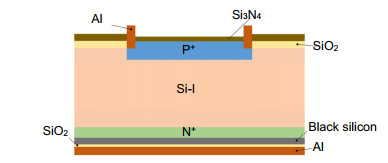
图 1 基于黑硅微结构的全硅PIN光电探测器横截面示意图
Figure 1. Cross-sectional schematic diagram of an all-silicon PIN photodetector based on the black silicon microstructure
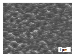
图 2 黑硅微结构层电镜扫描图
Figure 2. Scanning electron microscope image of the black silicon microstructure layer
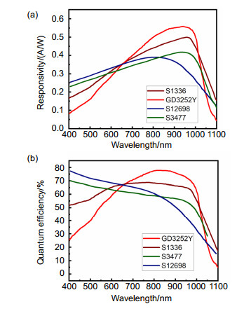
图 3 基于黑硅微结构的硅PIN光电探测器GD3252Y与常规PIN光电探测器光谱响应和量子效率的对比曲线
Figure 3. Comparison curves of spectral response and quantum efficiency between silicon PIN photodetector GD3252Y based on the black silicon microstructure and the conventional PIN photodetector
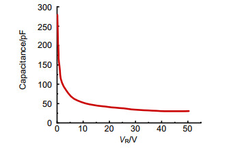
图 4 基于黑硅微结构的全硅PIN光电探测器电容特性曲线
Figure 4. Capacitance characteristic curve of the all-silicon PIN photodetector based on black silicon microstructure
表 1 基于黑硅微结构的PIN光电探测器的光电特性(Ta=23 ℃)
Table 1. Photoelectric characteristics of the PIN photodetector based on the black silicon microstructure(Ta=23 ℃)
Parameter Test conditions Typical value Photosensitive area size (A) 5.8 mm×5.8 mm Spectral response range (λ) 400 nm~1100 nm Rise time (tr) VR=10 mV 200 ns Dark current (ID) VR=10 mV 700 pA Capacitance (Cj) F=10 MHz
VR=10 mV280 pF Reverse voltage (VR) 10 mV  下载: 导出CSV
-
参考文献
[1] Yin T, Cohen R, Morse M M, et al. 31 GHz Ge n-i-p waveguide photodetectors on Silicon-on-Insulator substrate[J]. Opt Express, 2007, 15(21): 13965-13971. doi: 10.1364/OE.15.013965
[2] Virot L, Benedikovic D, Szelag B, et al. Integrated waveguide PIN photodiodes exploiting lateral Si/Ge/Si heterojunction[J]. Opt Express, 2017, 25(16): 19487-19496. doi: 10.1364/OE.25.019487
[3] Benedikovic D, Virot L, Aubin G, et al. 25 Gbps low-voltage hetero-structured silicon-germanium waveguide pin photodetectors for monolithic on-chip nanophotonic architectures[J]. Photonics Res, 2019, 7(4): 437-444. doi: 10.1364/PRJ.7.000437
[4] Chen H, Verheyen P, De Heyn P, et al. Dark current analysis in high-speed germanium p-i-n waveguide photodetectors[J]. J Appl Phys, 2016, 119(21): 213105. doi: 10.1063/1.4953147
[5] Chen H, Verheyen P, De Heyn P, et al. -1 V bias 67 GHz bandwidth Si-contacted germanium waveguide p-i-n photodetector for optical links at 56 Gbps and beyond[J]. Opt Express, 2016, 24(5): 4622-4631. doi: 10.1364/OE.24.004622
[6] Cho H M, Barber W C, Ding H J, et al. Characteristic performance evaluation of a photon counting Si strip detector for low dose spectral breast CT imaging[J]. Med Phys, 2014, 41(9): 091903. doi: 10.1118/1.4892174
[7] Vaseashta A, Khudaverdyan S. Advanced Sensors for Safety and Security[M]. Dordrecht: Springer, 2013.
[8] Ho C K, Robinson A, Miller D R, et al. Overview of sensors and needs for environmental monitoring[J]. Sensors, 2005, 5(2): 4-37. doi: 10.1109/JSEN.2005.846481
[9] Menon P S, Shaari S. Surface versus lateral illumination effects on an interdigitated Si planar PIN photodiode[J]. Proc SPIE, 2005, 5881: 58810S. doi: 10.1117/12.616283
[10] Tasirin S K, Menon P S, Ahmad I, et al. High performance silicon lateral PIN photodiode[J]. IOP Conf Ser: Earth Environ Sci, 2013, 16: 012032. doi: 10.1088/1755-1315/16/1/012032
[11] Her T H, Finlay R J, Wu C, et al. Microstructuring of silicon with femtosecond laser pulses[J]. Appl Phys Lett, 1998, 73(12): 1673-1675. doi: 10.1063/1.122241
[12] Wu C, Crouch C H, Zhao L, et al. Near-unity below-band-gap absorption by microstructured silicon[J]. Appl Phys Lett, 2001, 78(13): 1850-1852. doi: 10.1063/1.1358846
[13] Savin H, Repo P, von Gastrow G, et al. Black silicon solar cells with interdigitated back-contacts achieve 22.1% efficiency[J]. Nat Nanotechnol, 2015, 10(7): 624-628. doi: 10.1038/nnano.2015.89
[14] Winkler M T, Sher M J, Lin Y T, et al. Studying femtosecond-laser hyperdoping by controlling surface morphology[J]. J Appl Phys, 2012, 111(9): 093511. doi: 10.1063/1.4709752
[15] Crouch C H, Carey J E, Shen M, et al. Infrared absorption by sulfur-doped silicon formed by femtosecond laser irradiation[J]. Appl Phys A, 2004, 79(7): 1635-1641. doi: 10.1007/s00339-004-2676-0
[16] Sher M J. Intermediate band properties of femtosecond-laser hyperdoped silicon[D]. Cambridge, Massachusetts: Harvard University, 2013.
[17] Baker‐Finch S C, Mcintosh K R. Reflection distributions of textured monocrystalline silicon: implications for silicon solar cells[J]. Prog Photovolt, 2013, 21(5): 960-971.
[18] Peng K Q, Xu Y, Wu Y, et al. Aligned single-crystalline Si nanowire arrays for photovoltaic applications[J]. Small, 2005, 1(11): 1062-1067. doi: 10.1002/smll.200500137
[19] Shen M Y, Crouch C H, Carey J E, et al. Femtosecond laser-induced formation of submicrometer spikes on silicon in water[J]. Appl Phys Lett, 2004, 85(23): 5694-5696. doi: 10.1063/1.1828575
[20] Hamamatsu Photonicas. Silicon photodiode S1336-8BK[EB/OL]. [2021-01-12]. http://www.hamamatsu.com.cn/product/17585.html.
[21] Hamamatsu Photonicas. Silicon photodiode S3477-04[EB/OL]. [2021-01-12]. http://www.hamamatsu.com.cn/product/17626.html.
[22] Hamamatsu Photonicas. Silicon photodiode S12698-02[EB/OL]. [2021-01-12]. http://www.hamamatsu.com.cn/product/18699.html.
-
访问统计
 点击扫一扫
点击扫一扫
图(4)
表(1)
计量
- 文章访问数:
- PDF下载数:
- 施引文献: 0


