
 E-mail Alert
 RSS
RSS
Transmission properties of metal photonic crystal films in visible light and microwave
-
摘要
一维金属光子晶体薄膜是由金属-介质多层结构组成的等效均匀的各向异性超构材料。相比单层金属膜层,该结构在色散调控方面具有更多的自由度。在该结构中由于表面等离子体激元(SPP)的存在,可实现倏逝波的定向传输。在本文中,等效介质理论、时域有限元差分法(FDTD)的计算结果和实验结果都表明,传输倏逝波的波长、频宽和强度可通过金属光子晶体结构调整实现主动设计。金属膜厚比例越小,传输波长的中心和截止波长越长,频带越宽。当金属膜层厚度小于SPP穿透深度时,可获得宽频段的倏逝波的传输。同时,对金属光子晶体在微波波段的传输性能也进行了研究,发现其在微波波段等效介电常数为负,具有良好的反射性能。该结构的屏蔽效能远大于厚度相近的ITO薄膜的电磁屏蔽效能。在厚度只有几百纳米时,该结构即可实现良好的电磁屏蔽效能。通过金属光子晶体薄膜可实现电磁屏蔽材料的薄膜化、轻质化和可视化。

Abstract
The one-dimensional metallic photonic crystal film is an anisotropic metamaterial with an equivalent and uniform metal-medium multilayered structure. Compared with the single-layer metal film, the one-dimensional metal photonic crystal film has a higher degree of freedom in terms of chromatic dispersion regulation and control. With the existing of surface plasmon polariton (SPP), directional transmission of evanescent waves can be achieved. The experimental results and the calculated results of the equivalent medium theory and the finite-difference time domain (FDTD) method show that the active control on the wavelength, bandwidth and strength of the evanescent waves during transmitting can be realized by regulating the metal photonic crystal structure. The smaller is the ratio of metal film thickness, the longer are the center of the transmission wavelength and the cutoff wavelength, and the wider is the frequency band. When the thickness of the metal film layer is smaller than the penetration depth of the SPP, wide frequency-band evanescent waves can be transmitted. This paper also studied the transmission performance in the microwave band of the metal photonic crystal, finding that at the microwave band, the equivalent dielectric constant of the metal photonic crystal is negative and the metallic photonic crystal has a good reflection property. Furthermore, the shielding effectiveness of the metal photonic crystal film is far better than the electromagnetic shielding effectiveness of the ITO film with the same thickness. Even at the thickness of a few hundred of nanometers, the metallic photonic crystal film can achieve good electromagnetic shielding effectiveness. Thus, by adopting the metallic photonic crystal film, light and visual electromagnetic shielding materials with thin films can be created.
-
Overview

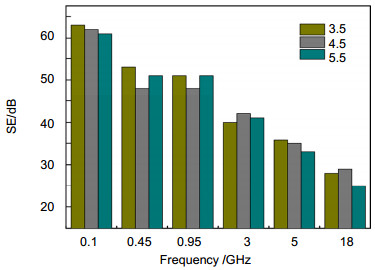
Abstract: The one-dimensional metallic photonic crystal film is an anisotropic metamaterial with an equivalent and uniform metal-medium multilayered structure. Compared with single-layer metal film, the one-dimensional metal photonic crystal film has a higher degree of freedom in terms of chromatic dispersion regulation and control. With the existing of surface plasmon polariton (SPP), directional transmission of evanescent waves can be achieved. This paper designed a one-dimensional metallic photonic crystal film, which was made of ITO and Ag layers. The thickness of each Ag films is less than 2 times the penetration depth of SPP. According to the effective medium theory of metallic photonic crystal, it is found that the equivalent dielectric constant of metallic photonic crystal structure in visible region can be greater than 0 by structural adjustment and its equivalent dielectric constant can be negative in microwave region. This makes metallic photonic crystal in visible region have higher transmitting performance due to the SPP coupling effect, as shown in Fig.(a). In infrared and microwave bands, due to the band gap, metallic photonic crystal shows good reflectivity (shielding effectiveness) in Fig.(b). Based on the effective medium theory, both FDTD and experimental results showed that, in metallic photonic crystal, lower metal component ratio corresponds to greater cutoff wavelength and center wavelength in visible light, wider transmission frequency band, and lower electromagnetic shielding effectiveness in microwave band. Results in this paper agreed with the SPP mode coupling theory, by which active design of transmission performance in visible light and electromagnetic shielding effectiveness in microwave band for metallic photonic crystal is possible. Additionally, the research shows that thinner metallic film layer corresponds to stronger SPP coupling effect and transmittance of visible light. When the metallic film thickness is less than the penetration depth of SPP, visible light transmission in wide frequency band can be achieved due to the smaller distance between the spacing of modes. Furthermore, when the pairs of metallic photonic crystal are 3.5, a good forbidden band can be well formed. With further increase of its pairs, no increase can be seen in the shielding performance of the metallic photonic crystal film. In conclusion, metallic photonic crystal film can be used to realize efficient transmission of visible light, and it also supports the active design of center wavelength, cutoff wavelength and bandwidth for the transmission of visible light. Thus, by adopting the metallic photonic crystal film, light and visual electromagnetic shielding materials with thin films can be created. This unique feature makes the metallic photonic crystal have wide application prospects in the field of visible electromagnetic shielding.
-

-
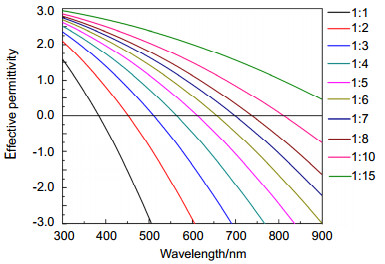
图 2 含不同金属Ag和ITO膜厚比例的等效介电常数.
Figure 2. Calculated effective permittivity for different thickness ratios of Ag and ITO films.
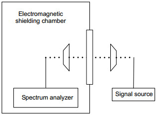
图 3 屏蔽室法测试材料屏蔽效能的方法.
Figure 3. Method for testing shielding effectiveness by shielding chamber.
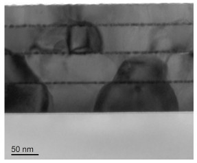
图 4 (ITO(60 nm)Ag(15 nm))3ITO(60 nm)样品的TEM形貌图.
Figure 4. TEM images of (ITO(60 nm)Ag(15 nm))3ITO (60 nm).
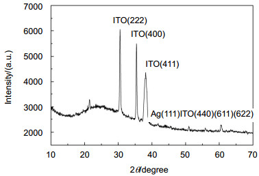
图 5 (ITO(60 nm)Ag(15 nm))3ITO(60 nm)样品的XRD图.
Figure 5. X-ray diffraction spectrum of (ITO(60 nm)Ag(15 nm))3 ITO(60 nm).
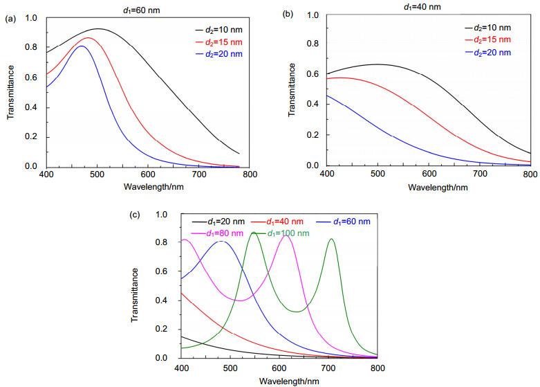
图 6 不同结构的金属光子晶体可见光透光率. (a) ITO膜层厚度为60 nm时不同金属膜厚的可见光透光率. (b) ITO膜层厚度为40 nm时, 不同金属膜厚的可见光透光率. (c) Ag膜厚为20 nm,不同ITO膜层厚度下可见光透光率.
Figure 6. Optical transmission spectra for samples with different structures. (a) Optical transmission spectra for samples with different thickness of Ag films and a fixed 60 nm ITO film. (b) Optical transmission spectra for samples with different thickness of Ag films and a fixed 40 nm ITO film. (c) Optical transmission spectra for samples with different thickness of ITO films and a fixed 20 nm Ag film.

图 7 在ITO膜层厚度为60 nm,周期数为3.5,金属Ag膜厚为4 nm、6 nm和8 nm样品的可见光透光率.
Figure 7. Optical transmission spectra for samples consisted of 3.5 pairs with 4 nm, 6 nm, 8 nm Ag films, respectively and a fixed 60 nm ITO film.
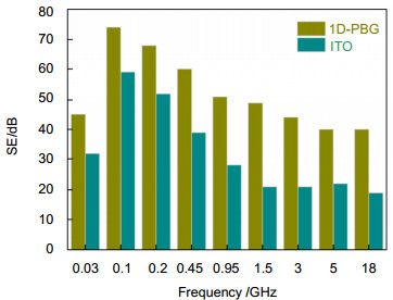
图 8 (ITO(60 nm)Ag(22 nm))3ITO(60 nm)一维金属光子晶体薄膜(1D-PBG)及300 nm膜厚的ITO薄膜的电磁屏蔽性能.
Figure 8. Electromagnetic shielding effectiveness for samples with structure of (ITO(60 nm)Ag(22 nm))3ITO(60 nm) and ITO films with a thickness of 300 nm.
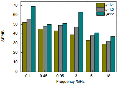
图 9 周期数为3.5,每层ITO膜厚为40 nm时,在不同金属膜厚比例下金属光子晶体薄膜的电磁屏蔽性能.
Figure 9. Electromagnetic shielding effectiveness for samples with 3.5 pairs of Ag/ITO consisted of different thickness ratio of Ag films, respectively and a fixed 40 nm ITO film.
-
参考文献
[1] Barnes W L, Dereux A, Ebbesen T W. Review article surface plasmon subwavelength optics[J]. Nature, 2004, 424(6950): 424-830. https://www.hanspub.org/reference/ReferencePapers.aspx?ReferenceID=5829&&PaperID=11925
[2] Jena S, Tokas R B, Sarkar P, et al. Omnidirectional photonic band gap in magnetron sputtered TiO2/SiO2 one dimensional photonic crystal[J]. Thin Solid Films, 2016, 599: 138-144. doi: 10.1016/j.tsf.2015.12.069
[3] Shen Huaizhong, Wang Zhanhua, Wu Yuxin, et al. One-dimen sional photonic crystals: fabrication, responsiveness and emerging applications in 3D construction[J]. RSC Advances, 2015, 6(6): 4505-4520. http://cn.bing.com/academic/profile?id=e1991cb0b1b6c89b4f2bb1d295cf622e&encoded=0&v=paper_preview&mkt=zh-cn
[4] Moslemi F, Jamshidi-Ghaleh K. Electrically tunable optical bistability based on one-dimensional photonic crystals with nonlinear nanocomposite materials[J]. Journal of Applied Physics, 2016, 119(9): 093101. doi: 10.1063/1.4942866
[5] Xiao Xing, Wang Wenjun, Li Shuhong, et al. Investigation of defect modes with Al2O3 and TiO2 in one-dimensional photonic crystals[J]. Optik, 2015, 127(1): 135-138. https://www.sciencedirect.com/science/article/pii/S0030402615013601
[6] Degli-Eredi I, Sipe J E, Vermeulen N. TE-polarized graphene modes sustained by photonic crystal structures[J]. Optics Letters, 2015, 40(9): 2076-2079. doi: 10.1364/OL.40.002076
[7] Luo Zhaoming, Chen Min, Deng Jiyuan, et al. Low-pass spatial filters with small angle-domain bandwidth based on one-dimensional metamaterial photonic crystals[J]. Optik, 2015, 127(1): 259-262. http://or.nsfc.gov.cn/bitstream/00001903-5/346801/1/1000014329657.pdf
[8] Liu Yongqi, Qi Xinyuan, Lu Yang, et al. Observation of beam deflection in one-dimensional photonic lattice in LiNbO3 crystal accompanied with self-focusing and self-defocusing nonlinearities[J]. Physics Letters A, 2016, 380(1-2): 322-325. doi: 10.1016/j.physleta.2015.10.025
[9] Xiao Xuyang, Chen Runping. Study of omnidirectional reflection bandgap extension in one-dimensional quasi-periodic metallic photonic crystal[J]. Nano, 2015, 10(6): 1550088. doi: 10.1142/S1793292015500885
[10] Pavlichenko I, Broda E, Fukuda Y, et al. Bringing one-dimen sional photonic crystals to a new light: an electrophotonic platform for chemical mass transport visualisation and cell monitoring[J]. Materials Horizons, 2015, 2(3): 299-308. doi: 10.1039/C4MH00195H
[11] Yu Wenjuan, Jia Xu, Long Yongbing, et al. Highly efficient semitransparent polymer solar cells with color rendering index approaching 100 using one-dimensional photonic crystal[J]. ACS Applied Materials & Interfaces, 2015, 7(18): 9920-9928. http://cn.bing.com/academic/profile?id=2ca09dc0ed87d99dd87e8e85faf65e18&encoded=0&v=paper_preview&mkt=zh-cn
[12] Mandal S, Bose C, Bose M K. A generalized design of one dimensional photonic crystal based optical filter with lossy materials[J]. Optical and Quantum Electronics, 2016, 48(3): 200. doi: 10.1007/s11082-016-0460-y
[13] Aly A H, Ryu S W, Hsu H T, et al. THz transmittance in one-dimensional superconducting nanomaterial-dielectric sup erlattice[J]. Materials Chemistry and Physics, 2009, 113(1): 382-384. doi: 10.1016/j.matchemphys.2008.07.123
[14] Sigalas M M, Chan C T, Ho K M, et al. Metallic photonic band-gap materials[J]. Physical Review B, 1995, 52(16): 11744-11751. doi: 10.1103/PhysRevB.52.11744
[15] 郭迎辉, 蒲明博, 马晓亮, 等.电磁超构材料色散调控研究进展[J].光电工程, 2017, 44(1): 3-22. http://www.oejournal.org/J/OEE/Article/Details/A170317000570/CN
Guo Yinghui, Pu Mingbo, Ma Xiaoliang, et al. Advances of dispersion-engineered metamaterials[J]. Opto-Electronic Engineering, 2017, 44(1): 3-22. http://www.oejournal.org/J/OEE/Article/Details/A170317000570/CN
[16] 叶卫民.光子晶体导论[M].北京:科学出版社, 2010: 233-234.
Ye Weimin. Introduction of Photonic Crystals[M]. Beijing: Science Press, 2010: 233-234
[17] Scalora M, Bloemer M J, Pethel A S, et al. Transparent, metallo-dielectric, one-dimensional, photonic band-gap structures[J]. Journal of Applied Physics, 1998, 83(5): 2377-2383. doi: 10.1063/1.366996
[18] Aly A H, Ismaeel M, Abdel-Rahman E. Comparative study of the one dimensional dielectric and metallic photonic crystals[J]. Optics and Photonics Journal, 2012, 2(2): 105-112. doi: 10.4236/opj.2012.22014
[19] 叶卫民.光子晶体导论[M].北京:科学出版社, 2010: 40.
Ye Weimin. Introduction of Photonic Crystals[M]. Beijing: Science Press, 2010: 40.
[20] Oskooi A F, Roundy D, Ibanescu M, et al. MEEP: a flexible free-software package for electromagnetic simulations by the FDTD method[J]. Computer Physics Communications, 2010, 181(3): 687-702. doi: 10.1016/j.cpc.2009.11.008
[21] Wood B, Pendry J B, Tsai D P. Directed subwavelength imaging using a layered metal-dielectric system[J]. Physical Review B, 2006, 74(11): 115116. doi: 10.1103/PhysRevB.74.115116
[22] Belov P A, Hao Yang. Subwavelength imaging at optical frequencies using a transmission device formed by a periodic layered metal-dielectric structure operating in the canalization regime[J]. Physical Review B, 2006, 73(11): 113110. doi: 10.1103/PhysRevB.73.113110
[23] Cai Wenshan, Shalaev V. Optical metamaterials: fundamentals and applications[M]. New York: Springer-Verlag, 2010: 123- 136.
[24] Pradhan S K, Xiao Bo, Skuza J R, et al. Effects of dielectric thickness on optical behavior and tunability of one-dimensional Ag/SiO2 multilayered metamaterials[J]. Optics Express, 2014, 22(10): 12486-12498. doi: 10.1364/OE.22.012486
-
访问统计
 下载:
下载:
 点击扫一扫
点击扫一扫

图(10)
计量
- 文章访问数:
- PDF下载数:
- 施引文献: 0


