
 E-mail Alert
 RSS
RSS
The investigation of focusing characteristic based on double Bowtie nano-lithography structure
-
摘要:
Bowtie孔径结构已被广泛用于纳米直写光刻领域来获得超衍射聚焦光斑。然而,利用该结构获得的超衍射聚焦光斑呈椭圆形,影响了Bowtie结构的进一步应用。为了获得超衍射且圆形对称的聚焦光斑,本文提出了双Bowtie新型纳米光刻结构并利用Comsol软件仿真模拟了该结构的焦斑对称特性和电场增强特性。结果表明利用双Bowtie结构获得了圆形对称焦斑,并且出射面的电场强度得到了增强,是入射面电场强度的22倍。本文进一步将双Bowtie结构与金属/介质/金属结构相结合,使得局域增强后的透射光的传输距离(工作距)得到了显著延长。

-
关键词:
- Bowtie孔径结构 /
- 纳米直写光刻 /
- 电场增强特性 /
- 金属/介质/金属结构
Abstract:Bowtie aperture has been widely applied in the realm of nanometer direct-writing lithography for obtaining focusing spots beyond the diffraction limit. However, the obtained spot is elliptic-shape for the Bowtie case, which impacts the applications of the Bowtie structure. Double Bowtie aperture, as a novel nano-lithography structure, is proposed to attain circle-symmetric focusing spots beyond diffraction limit. The results demonstrate that circle-symmetry spots can be obtained, and the electric field intensity of transmission light is 22 times of that of incidence. By combining the double Bowtie structure with metal-insulator-metal, the propagation length of the enhanced transmission light is obviously prolonged.
-

Abstract: The Bowtie aperture structure is widely applied in the realm of nanometer direct-writing lithography for obtaining the focusing spots beyond the diffraction limit. However, the shape of spots obtained is elliptic under the Bowtie structure because the electric field is enhanced and located only in perpendicular to the aperture gap. This characteristic impacts the applications of Bowtie structure. To attain high-resolution and circle-symmetric focusing spots, the double Bowtie structure is proposed. The electric field is enhanced and located in both x and y directions due to the symmetry characteristic of the double Bowtie aperture. The free electrons are accumulated at four tips of the gap of the double Bowtie aperture, which stimulate the localized surface plasmas (LSPs) and develop the double-dipole oscillation mode. This characteristic attributes to obtain circle-symmetry spots and enhance the electric field intensity of transmission light. The simulated results demonstrate that the electric field intensity of transmission light is 22 times than that of incidence. However, the electric field intensity of transmission light decays in the form of exponential with the increasing of the working distance.
The electric field intensity of transmission light decays with exponential perpendicularly to the interface of metal/insulator but still propagates parallel to interface as evanescent wave. The transmission light is coupled into the interface of metal/insulator by this electric field generated by the evanescent wave, and which further stimulates surface plasmas (SPs). The silver, as a common waveguide material, can enhance and magnify the evanescent wave. We combine the double Bowtie structure with metal-insulator-metal structure. Although the electric field intensity still decays with exponential, the electric field intensity attained keeps 1 time as large as that of incidence light when the distance approaches to 50 nm. The propagation distance of light is obviously prolonged which benefits from the characteristic of the transmission enhancement of the upper silver and the characteristic of reflection of the bottom silver.
Therefore, the double Bowtie aperture has an advantage in obtaining high-resolution and circle-symmetry spots. Metal/insulator/metal structure combined with the double Bowtie aperture further attributes to prolong the transmission distance of light. This advantage facilitates the applications of Bowtie structure in nanometer direct-writing lithography technology.
-

-
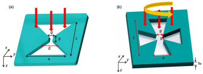
图 1 纳米光刻结构示意图. (a) Bowtie型结构. (b)双Bowtie结构.
Figure 1. Nano-lithography structure diagram. (a) Bowtie structure. (b) Double Bowtie structure.
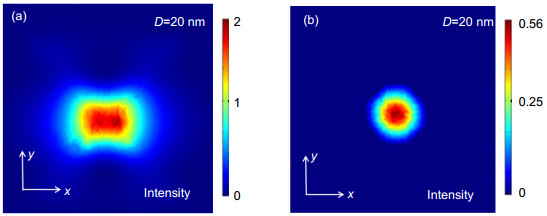
图 2 纳米光刻结构焦斑特性对比图. (a) Bowtie结构的焦斑特性. (b)双Bowtie结构的焦斑特性.
Figure 2. Contrast diagram of focused spots in (a) Bowtie structure and (b) double Bowtie structure.
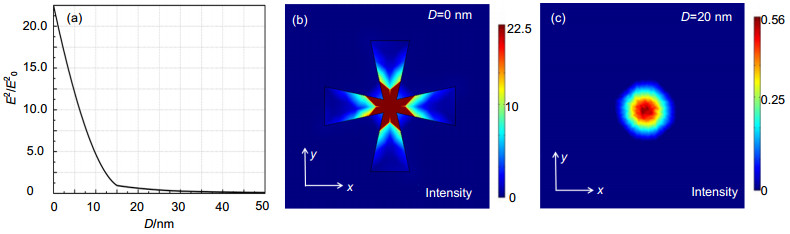
图 3 双Bowtie结构电场增强特性模拟结果. (a) E2/E02随工作距(D)的变化. (b) D=0处的电场强度分布. (c) D=20 nm处的电场强度分布.
Figure 3. Characteristic of electric enhancement in double Bowie structure with different distances. (a) The result of E2/E02 with working distance (b) D=0 nm, (c) D=20 nm.
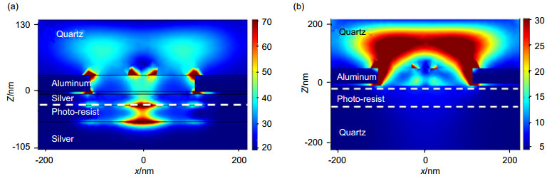
图 4 两种结构下记录介质中的总电场分布. (a)双Bowtie+MIM结构. (b)双Bowtie结构.
Figure 4. Distribution of total electric field intensity in (a) double Bowtie+Ag/Pr/Ag and (b) double Bowtie structures.
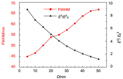
图 5 光刻胶中心处的E2/E02和FWHM随工作距(D)的变化.
Figure 5. Variation of E2/E02 and FWHM with the working distance (D) in the photoresist center.
表 1 双Bowtie结构参数列表.
Table 1. Parameters of double Bowtie structure.
Parameters Parameter size/nm L 200 a 60 g 30 tM 30  下载: 导出CSV
-
[1] Synge E H. A suggested method for extending microscopic resolution into the ultra-microscopic region[J]. The London, Edinburgh, and Dublin Philosophical Magazine and Journal of Science, 1928, 6(35): 356–362. doi: 10.1080/14786440808564615
[2] Shi Xiaolei, Hesselink Lambertus. Mechanisms for enhancing power throughput from planar nano-apertures for near-field optical data storage[J]. Japanese Journal of Applied Physics, 2002, 41(3B): 1632. http://cn.bing.com/academic/profile?id=b7701fe12618b6c6144a9868b218849c&encoded=0&v=paper_preview&mkt=zh-cn
[3] Tanaka K, Ohkubo T, Oumi M, et al. Simulation of simultaneous tracking/data signal detection using novel aperture-mounted surface recording head[J]. Japanese Journal of Applied Physics, 2002, 41(3B): 1628. http://cn.bing.com/academic/profile?id=405771c2235d03b7f999093ef9d1a70d&encoded=0&v=paper_preview&mkt=zh-cn
[4] Tanaka K, Tanaka M. Simulation of an aperture in the thick metallic screen that gives high intensity and small spot size using surface plasmon polariton[J]. Journal of Microscopy, 2003, 210(3): 294–300. doi: 10.1046/j.1365-2818.2003.01155.x
[5] Şendur K, Challener W. Near-field radiation of bow-tie antennas and apertures at optical frequencies[J]. Journal of Microscopy, 2003, 210(3): 279–283. http://onlinelibrary.wiley.com/doi/10.1046/j.1365-2818.2003.01145.x/full?globalMessage=0
[6] Wang L, Xu X. Spectral resonance of nanoscale bowtie apertures in visible wavelength[J]. Applied Physics A, 2007, 89(2): 293–297. doi: 10.1007/s00339-007-4125-3
[7] Jin Eric Xuan, Xu Xianfan. Finitte-difference time-domain studies on optical transmission through planar nano-apertures in a metal film[J]. Japanese Journal of Applied Physics, 2004, 43(1R): 407–417. http://cn.bing.com/academic/profile?id=a71f755ca89ae04c2cbfa4a10013e235&encoded=0&v=paper_preview&mkt=zh-cn
[8] Jin Eric Xuan, Xu Xianfan. Enhanced optical near field from a bowtie aperture[J]. Applied Physics Letters, 2006, 88(15): 153110– 153116. doi: 10.1063/1.2194013
[9] Kim S, Jung H, Kim Y, et al. Resolution limit in plasmonic lithography for practical applications beyond 2x-nm half pitch[J]. Advanced Materials, 2012, 24(44): OP337–OP344. http://cn.bing.com/academic/profile?id=c086a41cdae38a2b96ea7c1e3b4e312b&encoded=0&v=paper_preview&mkt=zh-cn
[10] Wang Yaohui, Yao Na, Zhang Wei, et al. Forming sub-32-nm high-aspect plasmonic spot via bowtie aperture combined with metal-insulator-metal scheme[J]. Plasmonics, 2015, 10(6): 1607–1613. doi: 10.1007/s11468-015-9966-6
[11] 王耀辉. 局域表面等离子体纳米直写光刻原理与方法研究[D]. 成都: 中国科学院光电技术研究所, 2015.
http://cdmd.cnki.com.cn/Article/CDMD-80151-1015951581.htm [12] 王耀辉, 何家玉, 王长涛, 等.增强型局域表面等离子体共振纳米直写光刻[J].光电工程, 2016, 43(1): 71–76. http://www.cqvip.com/QK/90982A/201601/667898213.html
Wang Yaohui, He Jiayu, Wang Changtao, et al. Method investigation of direct-writing nanolithography based on enhanced local surface plasmon resonance[J]. Opto-Electronic Engineering, 2016, 43(1): 71–76. http://www.cqvip.com/QK/90982A/201601/667898213.html
[13] 杨志林. 金属纳米粒子的光学性质及过渡金属表面增强拉曼散射的电磁场机理研究[D]. 厦门: 厦门大学, 2006.
http://cdmd.cnki.com.cn/Article/CDMD-10384-2007056510.htm [14] Palik E D. Handbook of optical constants of solids[M]. San Diego: Academic Press, 1998.
[15] Xu T, Fang L, Ma J, et al. Localizing surface plasmons with a metal-cladding superlens for projecting deep-subwavelength patterns[J]. Applied Physics B, 2009, 97(1): 175–179. doi: 10.1007/s00340-009-3615-8
-
 点击扫一扫
点击扫一扫
图(5)
表(1)
计量
- 文章访问数: 7302
- PDF下载数: 3067
- 施引文献: 0


