
 E-mail Alert
 RSS
RSS
Effect of oxygen partial pressure on amorphous Ga2O3-based solar-blind ultraviolet photodetectors
-
摘要:
非晶氧化镓(a-Ga2O3)基日盲紫外光电探测器的性能与a-Ga2O3薄膜内的氧空位有关,氧空位的浓度制约着探测器的响应度和响应速度。为了在探测器的响应度和响应速度之间达到平衡,本文通过微调射频磁控溅射过程中的氧分压,调控薄膜内的氧空位浓度,并在此基础上成功制备金属-半导体-金属(metal-semiconductor-metal,MSM)型日盲紫外探测器。研究结果显示,通过掺入氧气能减少薄膜内的氧空位,改善薄膜的致密度。适当条件的氧分压可以使探测器在维持良好响应度的前提下,同时拥有较快的响应速度,在两种互相制约的特性上达到了平衡。特别地,在3%氧分压条件下制备得到的日盲探测器在254 nm、80 μW/cm2的紫外光照射下具有2.6 A/W的响应度以及2.2 s/0.96 s的快速响应速度。
Abstract:Oxygen vacancies in the a-Ga2O3 film play a crucial role in the performance of a-Ga2O3-based solar-blind photodetectors (SBPDs). The concentration of oxygen vacancies is a “double-edged sword”, increasing the responsivity of the SBPDs but deteriorating the response speed. In order to achieve a balance between these two key parameters, we adjusted the oxygen vacancy concentration in the film by delicately tuning the oxygen partial pressure during the sputtering process. The metal-semiconductor-metal (MSM) SBPDs were prepared accordingly. The results demonstrate that incorporating moderate oxygen can reduce the oxygen vacancies in the film and improve the density of the film. Under appropriate conditions, the oxygen partial pressure enables the photodetector to maintain good responsivity while having a fast response speed. At an oxygen partial pressure of 3%, the device has a high responsivity of 2.62 A/W under 254-nm DUV irradiation and a fast response speed of 2.2 s/0.96 s.
-
Key words:
- a-Ga2O3 /
- solar-blind photodetector /
- responsivity /
- radio frequency magnetron sputtering
-
Overview: Solar-blind photodetectors(SBPDs) exhibit advantages such as high sensitivity, high communication accuracy, and high signal-to-noise ratio, making them highly desirable for applications in ozone hole monitoring, corona detection, missile warning, and other military and civil fields. Among the materials utilized for SBPDs, Ga2O3 is particularly attractive due to its bandgap that inherently corresponds to a solar-blind spectrum without any alloy and dopant. Generally, crystalline Ga2O3 exists in various polymorphs, including α, β, γ, ε, and δ. Among these, β-Ga2O3 possesses the most stable structure. Therefore, β-Ga2O3 in the form of thin films, nano-structures, and single crystals has been widely explored for detection applications. In 2018, Kanika et al. reported the growth of β-Ga2O3 thin films on silicon substrates using a high-temperature seed layer and successfully constructed a solar-blind UV photodetector. The device demonstrated excellent performance under extremely weak ultraviolet signals (44 nW/cm2) with a responsivity of 96.13 AW−1 and an external quantum efficiency of 4.76×10⁴. In 2019, Wang et al. prepared a high-quality β-Ga2O3 film on a sapphire substrate via magnetron sputtering followed by post-deposition annealing. Furthermore, a metal-semiconductor-metal(MSM) structure photodetector was successfully prepared. This device exhibited a photo-to-dark current ratio greater than 103, a response time of 0.31 s, and a decay time of 0.05 s. However, the high-temperature growth conditions required for β-Ga2O3 can increase the cost and complexity of the process, potentially hindering its widespread applications.
The amorphous Ga2O3 (a-Ga2O3), with its uniform structure, is getting popular among researchers worldwide, as it is fabricated through a simple process at low temperatures. As previously reported, a-Ga2O3-based photodetectors can obtain performance comparable to that of β-Ga2O3 photodetectors. Currently, radio frequency(RF) magnetron sputtering has been widely applied to prepare a-Ga2O3 thin films, which has the advantages of a fast growth rate, simplicity of operation, and low cost. However, despite the high responsivity of a-Ga2O3 solar-blind photodetectors prepared by RF magnetron sputtering, this high responsivity is often accompanied by a slow response speed. The reason for this is the presence of a large number of oxygen vacancies in the a-Ga2O3 films deposited via magnetron sputtering. In this paper, we optimized the oxygen partial pressure during magnetron sputtering to control the concentration of oxygen vacancies in the film. We prepared MSM photodetectors to investigate the effect of different oxygen partial pressures on the performance of the solar-blind photodetectors. The results demonstrate that the oxygen partial pressure can effectively regulate the oxygen vacancies in a-Ga2O3 thin films, and an optimized oxygen partial pressure allows the photodetector to achieve a balance between responsivity and response speed.
-

-
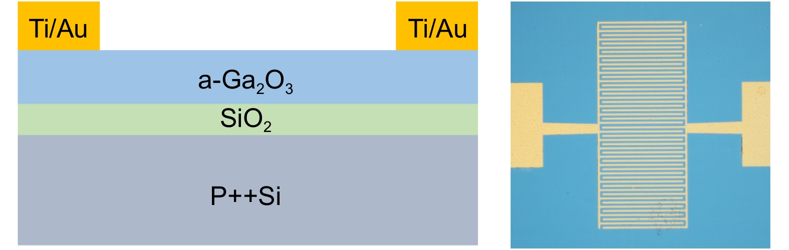
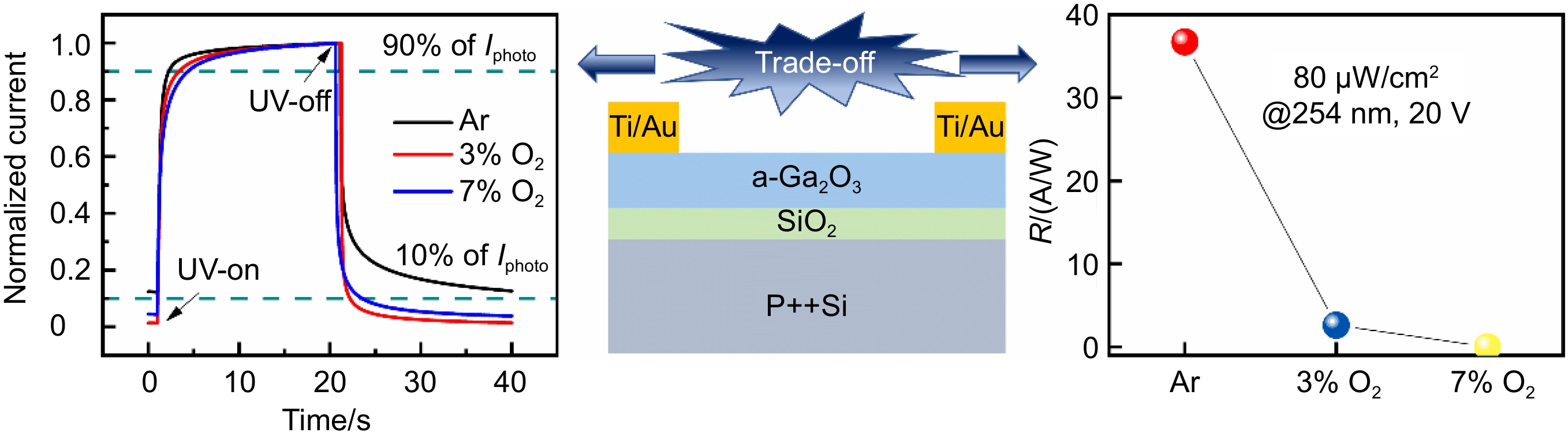
图 1 a-Ga2O3 MSM型日盲紫外探测器结构示意图(左)及其显微镜下实物图(右)
Figure 1. The schematic diagram of the a-Ga2O3 MSM SBPD (left) and its microscopic image (right)
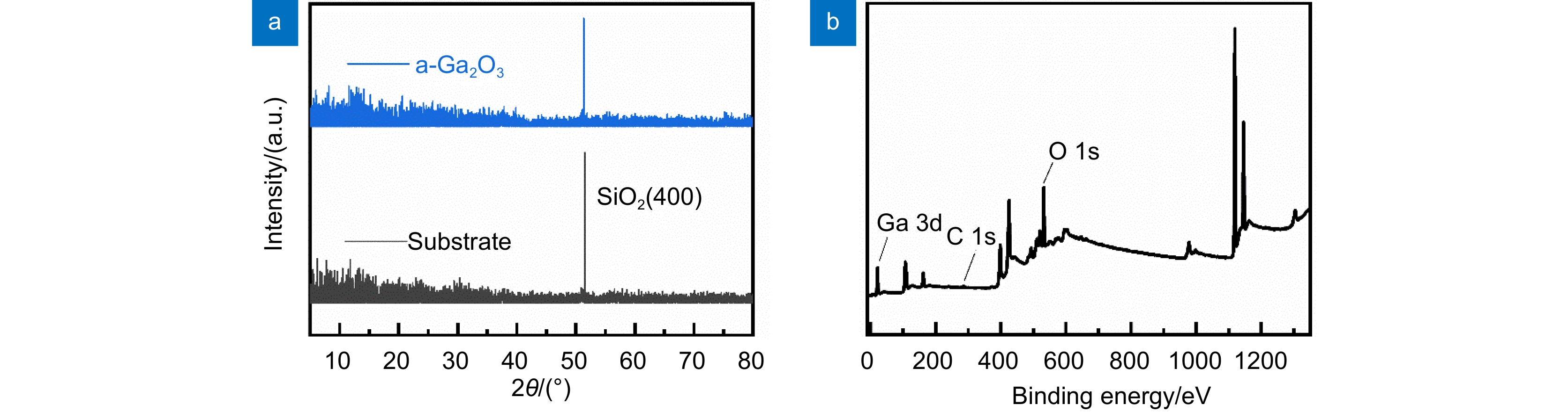
图 2 (a)纯氩条件下a-Ga2O3薄膜和衬底硅片的GIXRD θ~2θ扫描图谱;(b)纯氩条件下a-Ga2O3薄膜的XPS全谱
Figure 2. (a) GIXRD spectra of the substrate and a-Ga2O3 film deposited at pure Ar; (b) XPS survey of a-Ga2O3 film deposited at pure Ar
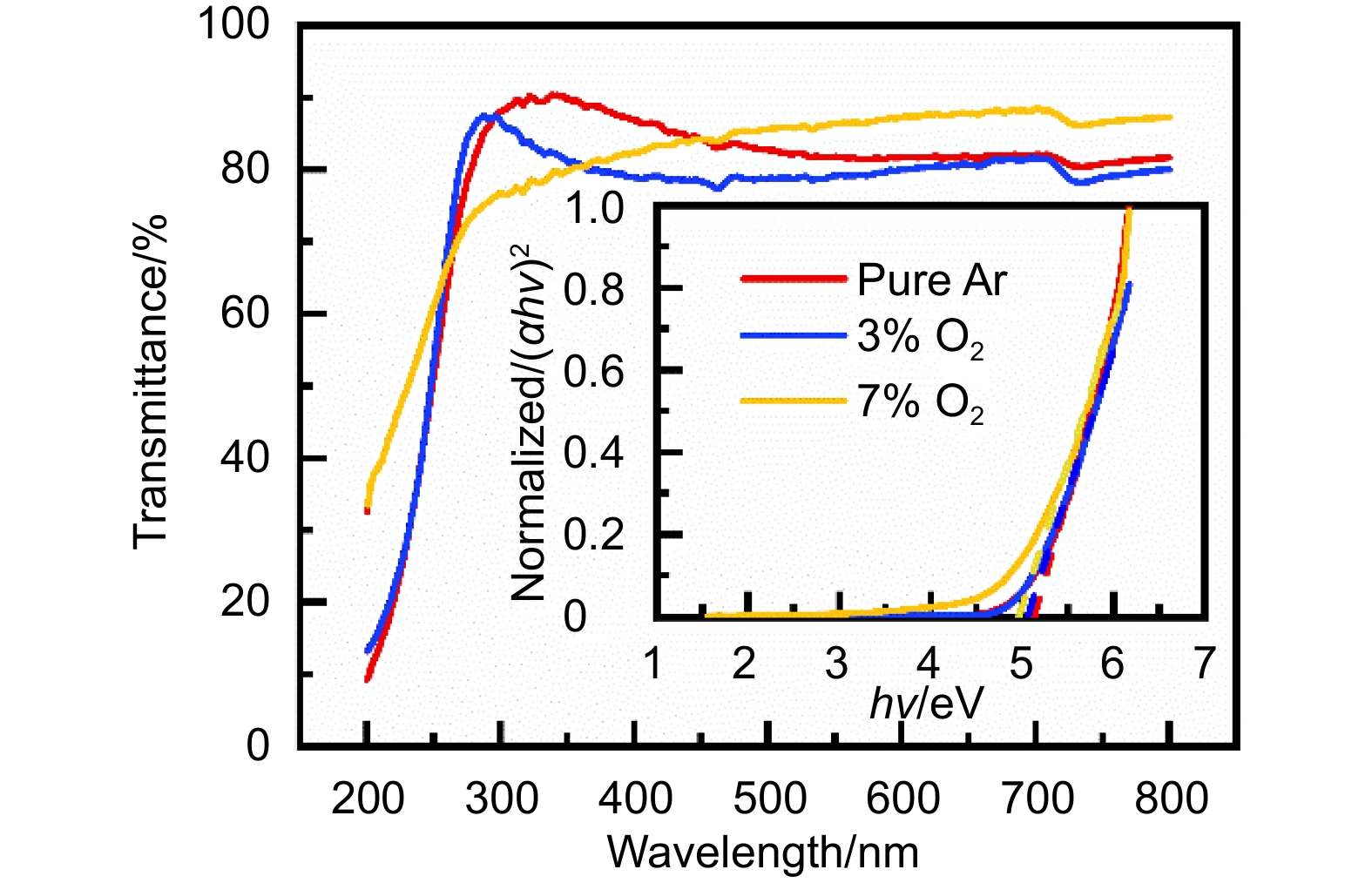
图 3 不同氧分压下a-Ga2O3薄膜的透射吸收光谱以及(αhν)2-hν曲线(插图)
Figure 3. Optical transmittance spectra of a-Ga2O3 films deposited at different oxygen partial pressures and (αhν)2-hν plots(inset)
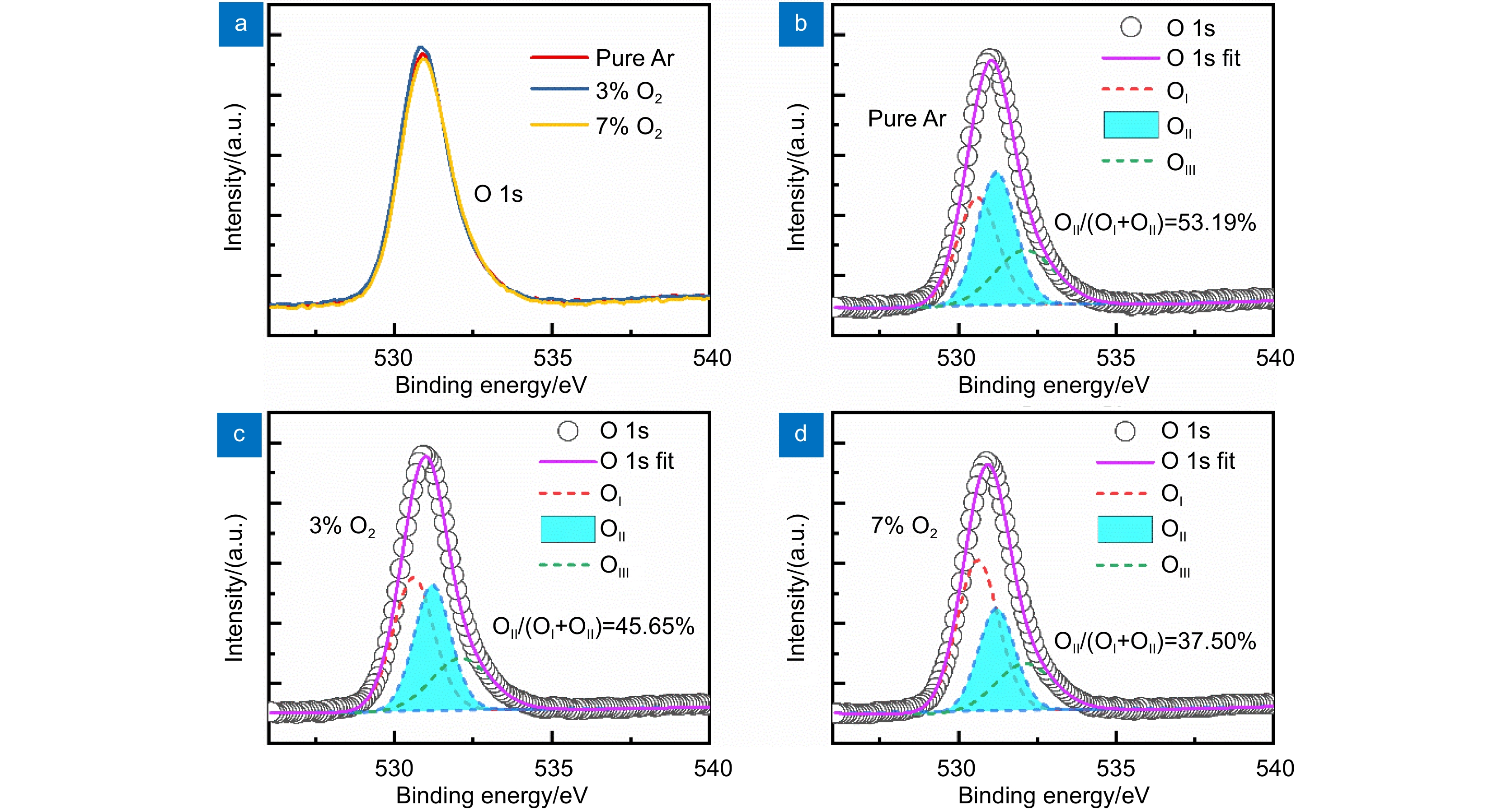
图 4 不同氧分压条件下a-Ga2O3薄膜的XPS O 1s峰位及拟合分峰结果。(a)不同氧分压下a-Ga2O3薄膜的XPS O 1s峰位;(b)纯氩;(c) 3%氧分压;(d) 7%氧分压条件下O 1s拟合分峰结果
Figure 4. XPS O 1s core level and fitting results of a-Ga2O3 films under different oxygen partial pressures. (a) O 1s core level of a-Ga2O3 films with different oxygen partial pressures; Fitting results of O 1s core level of (b) pure Ar, (c) 3% oxygen partial pressure, and(d) 7% oxygen partial pressure
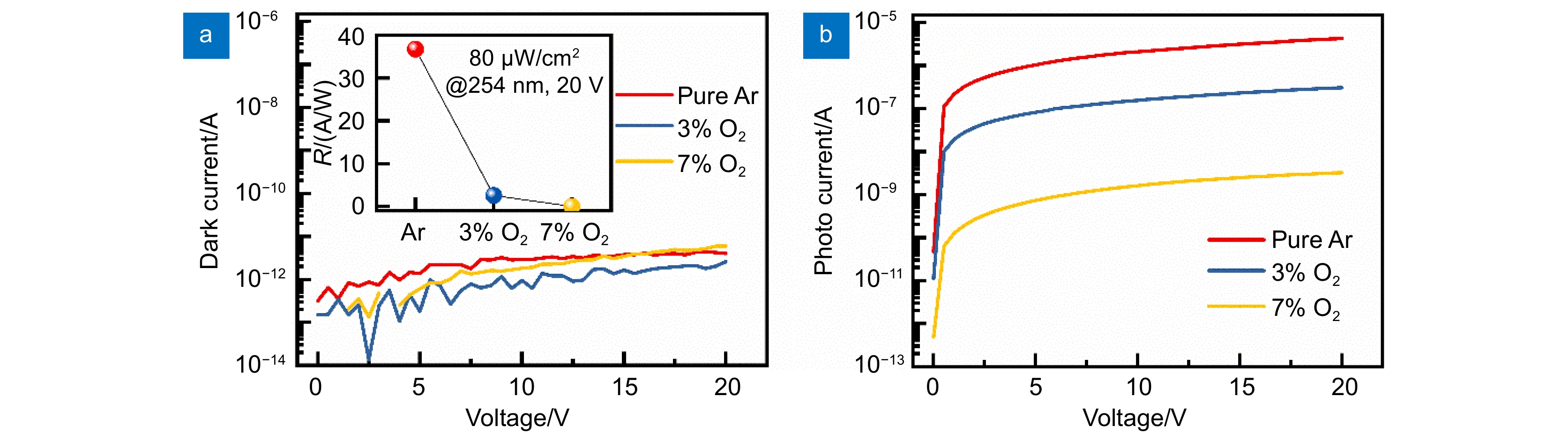
图 5 不同氧分压下a-Ga2O3 MSM型探测器的电流-电压特性曲线。(a)无紫外线光照下的电流电压曲线以及三个条件下的响应度(插图);(b) 254 nm、80 μW/cm2紫外光照下的电流电压曲线
Figure 5. The current-voltage(I-V) of the a-Ga2O3 MSM SBPDs under different oxygen partial pressures. (a) The dark current characteristics and the responsivity under three conditions(inset); (b) The photocurrent characteristics(254 nm, 80 μW/cm2)
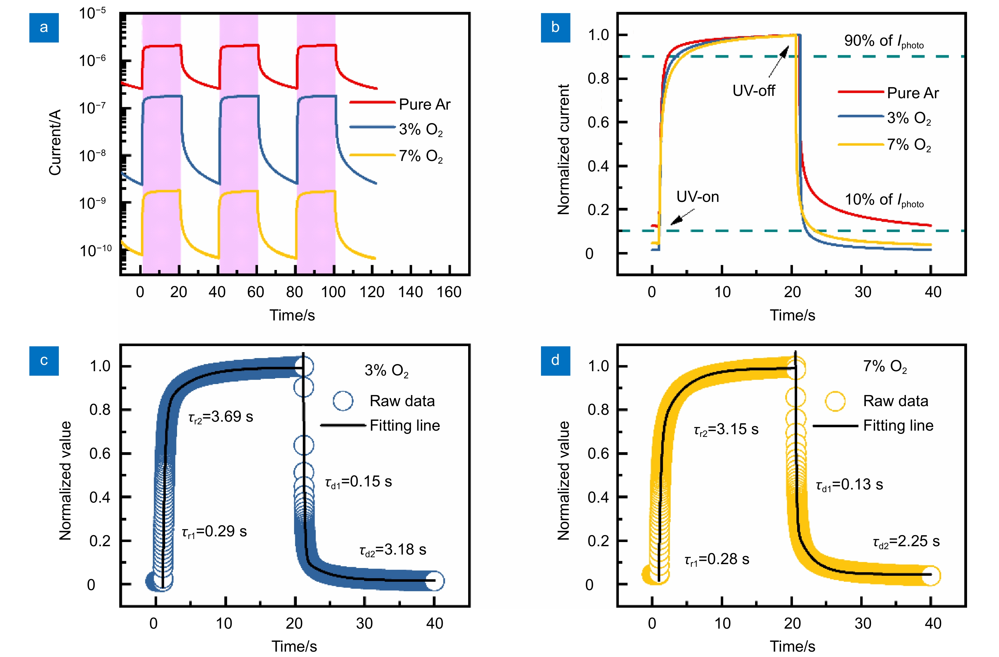
图 6 不同氧分压条件下a-Ga2O3 MSM型探测器的瞬态响应。(a)探测器多周期瞬态响应;(b)探测器单周期归一化瞬态响应;(c) 3%氧分压器件上升和下降过程的实验数据和拟合曲线;(d) 7%氧分压器件上升和下降过程的实验数据和拟合曲线
Figure 6. Transient responses of a-Ga2O3 MSM SBPDs under different oxygen partial pressures. (a) Transient response for multicycles; (b) Normalized transient response; Experimental and fitted curves of the rise and decay processes for the device with (c) 3% oxygen partial pressure and (d) 7% oxygen partial pressure
-
[1] Xu J J, Zheng W, Huang F. Gallium oxide solar-blind ultraviolet photodetectors: a review[J]. J Mater Chem C, 2019, 7(29): 8753−8770. doi: 10.1039/C9TC02055A
[2] 肖演, 杨斯铄, 程凌云, 等. 非晶氧化镓基日盲紫外探测器的研究进展[J]. 光电工程, 2023, 50(6): 230005. doi: 10.12086/oee.2023.230005
Xiao Y, Yang S S, Cheng L Y, et al. Research progress of solar-blind UV photodetectors based on amorphous gallium oxide[J]. Opto-Electron Eng, 2023, 50(6): 230005. doi: 10.12086/oee.2023.230005
[3] Qin Y, Long S B, Dong H, et al. Review of deep ultraviolet photodetector based on gallium oxide[J]. Chin Phys B, 2019, 28(1): 018501. doi: 10.1088/1674-1056/28/1/018501
[4] Xu Y, Cheng Y L, Li Z, et al. High performance gate tunable solar blind ultraviolet phototransistors based on amorphous Ga2O3 films grown by mist chemical vapor deposition[J]. Nano Select, 2021, 2(11): 2112−2120. doi: 10.1002/nano.202100029
[5] Wang Z, Zheng W, Hu Q C, et al. Pt/(InGa)2O3/n-Si heterojunction-based solar-blind ultraviolet photovoltaic detectors with an ideal absorption cutoff edge of 280 nm[J]. ACS Appl Mater Interfaces, 2021, 13(37): 44568−44576. doi: 10.1021/ACSAMI.1C13006
[6] Chen X, Liu K W, Wang X, et al. Performance enhancement of a ZnMgO film UV photodetector by HF solution treatment[J]. J Mater Chem C, 2017, 5(40): 10645−10651. doi: 10.1039/c7tc03352d
[7] Varshney U, Aggarwal N, Gupta G. Current advances in solar-blind photodetection technology: using Ga2O3 and AlGaN[J]. J Mater Chem C, 2022, 10(5): 1573−1593. doi: 10.1039/d1tc05101f
[8] Lu Y J, Lin C N, Shan C X. Optoelectronic diamond: growth, properties, and photodetection applications[J]. Adv Opt Mater, 2018, 6(20): 1800359. doi: 10.1002/adom.201800359
[9] Chen M N, Zhang Z P, Wen B, et al. Low dark current and high stability X-ray detector based on FAPbI3/Ga2O3 heterojunction[J]. J Alloys Compd, 2023, 941: 168989. doi: 10.1016/J.JALLCOM.2023.168989
[10] Arora K, Goel N, Kumar M, et al. Ultrahigh performance of self-powered β-Ga2O3 thin film solar-blind photodetector grown on cost-effective Si substrate using high-temperature seed layer[J]. ACS Photonics, 2018, 5(6): 2391−2401. doi: 10.1021/acsphotonics.8b00174
[11] Wang J, Ye L J, Wang X, et al. High transmittance β-Ga2O3 thin films deposited by magnetron sputtering and post-annealing for solar-blind ultraviolet photodetector[J]. J Alloys Compd, 2019, 803: 9−15. doi: 10.1016/j.jallcom.2019.06.224
[12] Lee S H, Kim S B, Moon Y J, et al. High-responsivity deep-ultraviolet-selective photodetectors using ultrathin gallium oxide films[J]. ACS Photonics, 2017, 4(11): 2937−2943. doi: 10.1021/acsphotonics.7b01054
[13] Qian L X, Wu Z H, Zhang Y Y, et al. Ultrahigh-responsivity, rapid-recovery, solar-blind photodetector based on highly nonstoichiometric amorphous gallium oxide[J]. ACS Photonics, 2017, 4(9): 2203−2211. doi: 10.1021/acsphotonics.7b00359
[14] Wang C, Fan W H, Zhang Y C, et al. Effect of oxygen flow ratio on the performance of RF magnetron sputtered Sn-doped Ga2O3 films and ultraviolet photodetector[J]. Ceram Int, 2023, 49(7): 10634−10644. doi: 10.1016/j.ceramint.2022.11.251
[15] Yang Y, Liu W M, Huang T T, et al. Low deposition temperature amorphous ALD-Ga2O3 thin films and decoration with MoS2 multilayers toward flexible solar-blind photodetectors[J]. ACS Appl Mater Interfaces, 2021, 13(35): 41802−41809. doi: 10.1021/acsami.1c11692
[16] Kobayashi E, Boccard M, Jeangros Q, et al. Amorphous gallium oxide grown by low-temperature PECVD[J]. J Vac Sci Technol, 2018, 36(2): 021518. doi: 10.1116/1.5018800
[17] Saikumar A K, Nehate S D, Sundaram K B. Review—RF sputtered films of Ga2O3[J]. ECS J Solid State Sci Technol, 2019, 8(7): Q3064−Q3078. doi: 10.1149/2.0141907jss
[18] Chen Y H, Han S, Yue D W, et al. UV response characteristics of amorphous Ga2O3 thin films with different microatom distributions and a low-temperature fabricated ultrahigh-performance a-Ga2O3 UV detector[J]. ACS Photonics, 2024, 11(3): 985−999. doi: 10.1021/acsphotonics.3c01311
[19] Kumar S S, Rubio E J, Noor-A-Alam M, et al. Structure, morphology, and optical properties of amorphous and nanocrystalline gallium oxide thin films[J]. J Phys Chem C, 2013, 117(8): 4194−4200. doi: 10.1021/jp311300e
[20] Ramana C V, Rubio E J, Barraza C D, et al. Chemical bonding, optical constants, and electrical resistivity of sputter-deposited gallium oxide thin films[J]. J Appl Phys, 2014, 115(4): 043508. doi: 10.1063/1.4862186
[21] Liao Y K, Jiao S J, Li S F, et al. Effect of deposition pressure on the structural and optical properties of Ga2O3 films obtained by thermal post-crystallization[J]. CrystEngComm, 2018, 20(1): 133−139. doi: 10.1039/C7CE01567D
[22] Wang Y H, Li H R, Cao J, et al. Ultrahigh gain solar blind avalanche photodetector using an amorphous Ga2O3-based heterojunction[J]. ACS Nano, 2021, 15(10): 16654−16663. doi: 10.1021/acsnano.1c06567
[23] Wang Y F, Lin Z H, Ma J L, et al. Multifunctional solar-blind ultraviolet photodetectors based on p-PCDTBT/n-Ga2O3 heterojunction with high photoresponse[J]. InfoMat, 2024, 6(2): e12503. doi: 10.1002/inf2.12503
[24] Liu Y M, Qin H Y, Peng C, et al. Boosting the responsivity of amorphous-Ga2O3 solar-blind photodetector via organosilicon surface passivation[J]. Appl Phys Lett, 2024, 124(8): 082102. doi: 10.1063/5.0184889
[25] Li Z, Feng Z Q, Xu Y, et al. High performance β-Ga2O3 solar-blind metal–oxide–semiconductor field-effect phototransistor with hafnium oxide gate dielectric process[J]. IEEE Electron Device Lett, 2021, 42(4): 545−548. doi: 10.1109/LED.2021.3061509
[26] Zhi Y S, Liu Z, Zhang S H, et al. 16 × 4 linear solar-blind UV photoconductive detector array based on β-Ga2O3 film[J]. IEEE Trans Electron Devices, 2021, 68(7): 3435−3438. doi: 10.1109/TED.2021.3081522
[27] Li X X, Zeng G, Li Y C, et al. High responsivity and flexible deep-UV phototransistor based on Ta-doped β-Ga2O3[J]. npj Flex Electron, 2022, 6(1): 47. doi: 10.1038/S41528-022-00179-3
[28] Cui S J, Mei Z X, Zhang Y H, et al. Room-temperature fabricated amorphous Ga2O3 high-response-speed solar-blind photodetector on rigid and flexible substrates[J]. Adv Opt Mater, 2017, 5(19): 1700454. doi: 10.1002/adom.201700454
[29] 石雄林, 刘宏宇, 候爽, 等. 表面等离子体在氧化镓基紫外探测器中的应用[J]. 光电工程, 2018, 45(2): 170728. doi: 10.12086/oee.2018.170728
Shi X L, Liu H Y, Hou S, et al. The applications of surface plasmons in Ga2O3 ultraviolet photodetector[J]. Opto-Electron Eng, 2018, 45(2): 170728. doi: 10.12086/oee.2018.170728
[30] 侯爽, 刘庆, 邢志阳, 等. Sn掺杂对Ga2O3基日盲紫外探测器性能的影响研究[J]. 光电工程, 2019, 46(10): 190011. doi: 10.12086/oee.2019.190011
Hou S, Liu Q, Xing Z Y, et al. Effects of Sn doping on Ga2O3-based solar blind photodetectors[J]. Opto-Electron Eng, 2019, 46(10): 190011. doi: 10.12086/oee.2019.190011
[31] Liu N S, Fang G J, Zeng W, et al. Direct growth of lateral ZnO nanorod UV photodetectors with schottky contact by a single-step hydrothermal reaction[J]. ACS Appl Mater Interfaces, 2010, 2(7): 1973−1979. doi: 10.1021/am100277q
-
 下载:
下载:
 点击扫一扫
点击扫一扫
图(7)
计量
- 文章访问数:
- PDF下载数:
- 施引文献: 0


