
 E-mail Alert
 RSS
RSS
The influence of active layer sputtering process and annealing temperature on the electrical properties of IZO TFT
-
摘要:
为了提高氧化物薄膜晶体管的器件性能,以掺In氧化锌(IZO)为有源层,原子层沉积法(ALD)沉积的Al2O3薄膜为栅介层,制备了基于IZO的薄膜晶体管(IZO TFT),研究了IZO薄膜制备工艺中溅射气体氩氧流量比、溅射压强和后退火温度等工艺参数对TFT器件电学性能的影响。结果表明,在恰当的氩氧比和反应气压以及相对较高的退火温度下制备的IZO TFT具有良好的电学特性,当氩氧流量比为60:20 sccm、溅射压强为0.5 Pa、空气气氛中以250 ℃退火1 h时后,IZO TFT器件的整体电学特性表现较优,其迁移率高达31 cm2/(V·s),开关电流比大于108。相对过低或过高的氩氧比会导致IZO有源层中氧空位含量过低或过高,从而降低TFT器件性能。过低的退火温度不足以使栅介质的Al-OH转变成Al-O以及空气中的氧扩散进入IZO体内钝化氧空位,因此器件性能较差。
Abstract:In order to improve the electrical performance of oxide thin film transistors, In-doped ZnO thin film transistors (IZO TFT) were prepared by using a sputtered IZO thin film as the active layer and an Al2O3 thin film deposited by atomic layer deposition (ALD) as the gate dielectric layer. The effects of the ratio of argon and oxygen, sputtering gas pressure, and annealing temperature on the electrical properties of IZO TFT were investigated during the IZO film preparation process. The results indicated that the IZO TFT, which was prepared at the appropriate argon-oxygen ratio and reaction pressure under relatively high annealing temperatures, shows excellent electrical characteristics. When the argon oxygen flow rate ratio was 60:20 sccm, the sputtering gas pressure was 0.5 Pa, and the air annealing temperature and time were 250 ℃ and 1 hour, respectively. The electrical properties of the IZO TFT were relatively better with a carrier saturation mobility of 31 cm2/(V·s) and a high on-off current ratio of 108. A relatively too-low or too-high argon-oxygen ratio could cause too-low or too-high oxygen vacancies in the active layer of IZO, thus reducing TFT device performance. The low annealing temperature couldn't transform the Al-OH bonds in the gate dielectric layer into Al-O bonds, and was difficult for oxygen in the air to diffuse into IZO and passivate oxygen vacancies, thus leading to poor device performance.
-
Key words:
- indium zinc oxide /
- thin film transistor /
- process parameters /
- electrical performance
-
Overview: In order to improve the electrical performance of oxide thin film transistors, In-doped ZnO thin film transistors (IZO TFT) were prepared by using a sputtered IZO thin film as the active layer and an Al2O3 thin film deposited by atomic layer deposition (ALD) as the gate dielectric layer. The effects of the ratio of argon and oxygen, sputtering gas pressure, and annealing temperature on the electrical properties of IZO TFT were investigated during the IZO film preparation process. The results indicated that the IZO TFT, which was prepared at the appropriate argon-oxygen ratio and reaction pressure under relatively high annealing temperatures, shows excellent electrical characteristics. When the argon oxygen flow rate ratio was 60:20 sccm, the sputtering gas pressure was 0.5 Pa, and the air annealing temperature and time were 250 ℃ and 1 hour, respectively. The electrical properties of the IZO TFT were relatively better with a carrier saturation mobility of 31 cm2/(V·s) and a high on-off current ratio of 108. A relatively too-low or too-high argon-oxygen ratio could cause too-low or too-high oxygen vacancies in the active layer of IZO, thus reducing TFT device performance. The low annealing temperature couldn't transform the Al-OH bonds in the gate dielectric layer into Al-O bonds, and was difficult for oxygen in the air to diffuse into IZO and passivate oxygen vacancies, thus leading to poor device performance. The IZO TFTs couldn't exhibit gate voltage control characteristics. When the annealing temperature was higher, it was beneficial to increase the density of IZO thin films, reduce the defect states inside and on the surface, and thus obtain high-performance IZO TFTs.
-

-
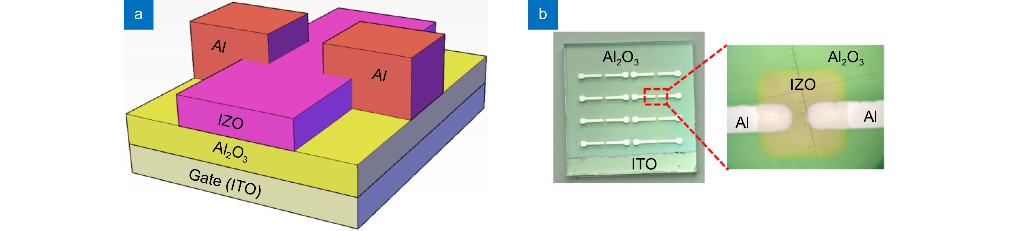
图 1 IZO TFT 器件图。(a)结构示意图;(b)实物拍照图
Figure 1. Structure and physical image of the IZO TFT. (a) Structure of the IZO TFT; (b) Physical image of the IZO TFT
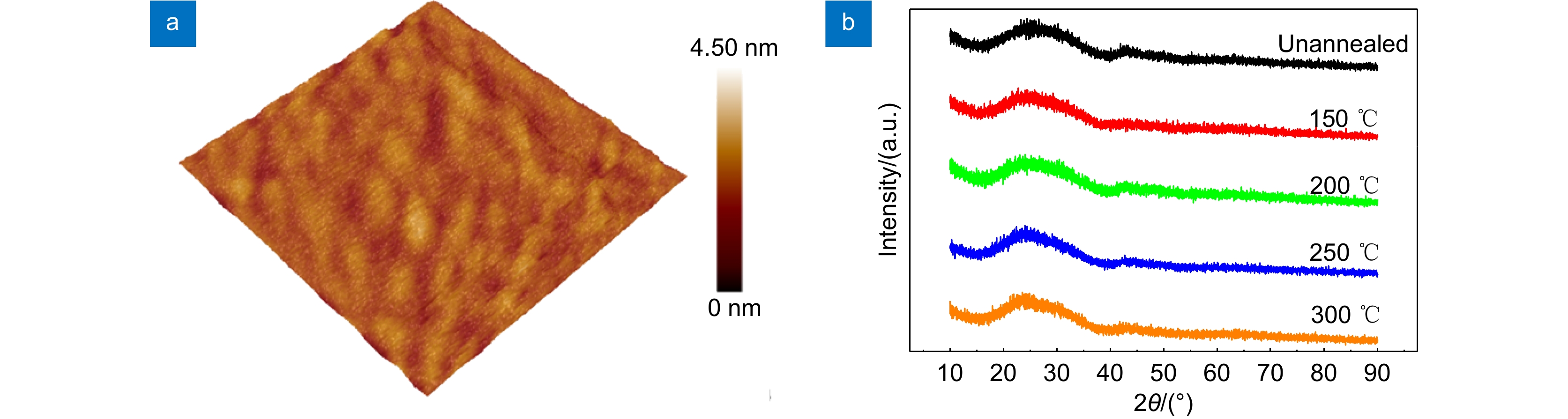
图 2 IZO薄膜的AFM图和XRD图。(a) AFM图;(b) XRD图
Figure 2. AFM and XRD images of the IZO thin films. (a) AFM; (b) XRD
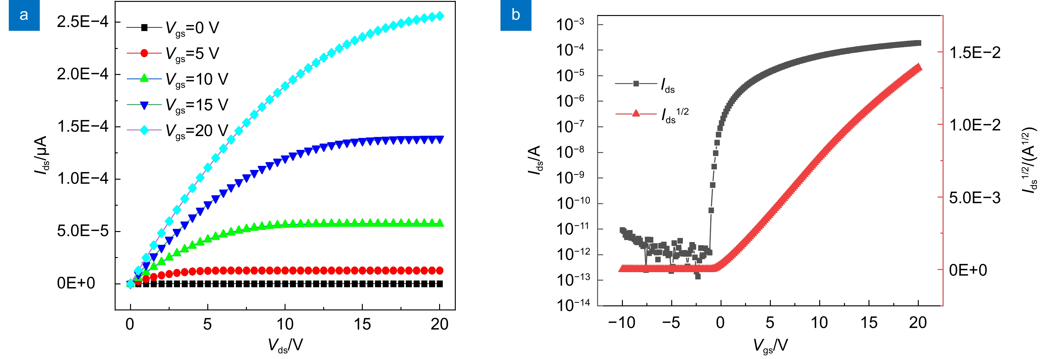
图 3 典型IZO TFT电学特性。(a)输出特性;(b)转移特性
Figure 3. Electrical properties of a type IZO TFT. (a) Output characteristics; (b) Transfer characteristics
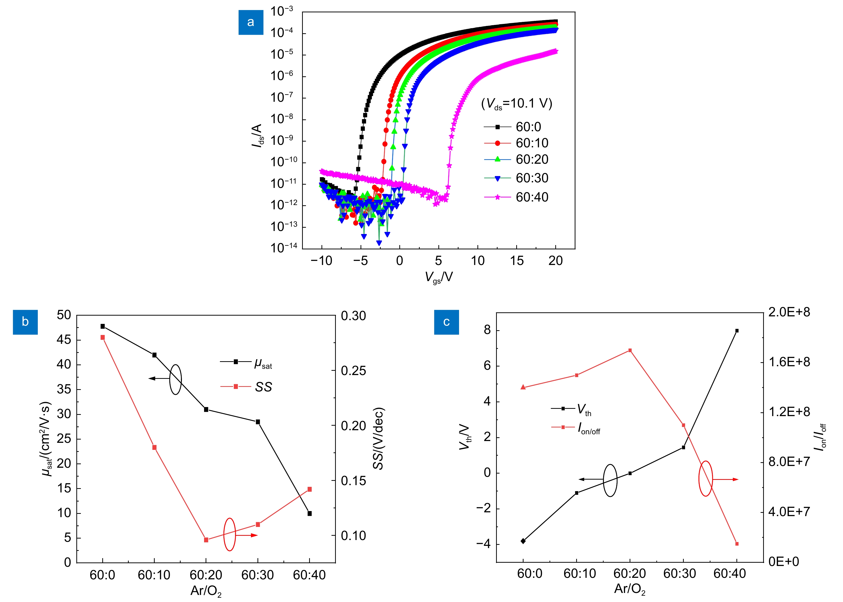
图 4 不同溅射氩氧流量比下制备的IZO TFT电学性能特性曲线。(a)转移特性;(b) µsat和SS;(c) Vth 和Ion/Ioff
Figure 4. Electrical characteristics of IZO TFT prepared at different ratios of argon to oxygen gas flow. (a) Transfer characteristics;(b) µsat and SS; (c) Vth and Ion/Ioff
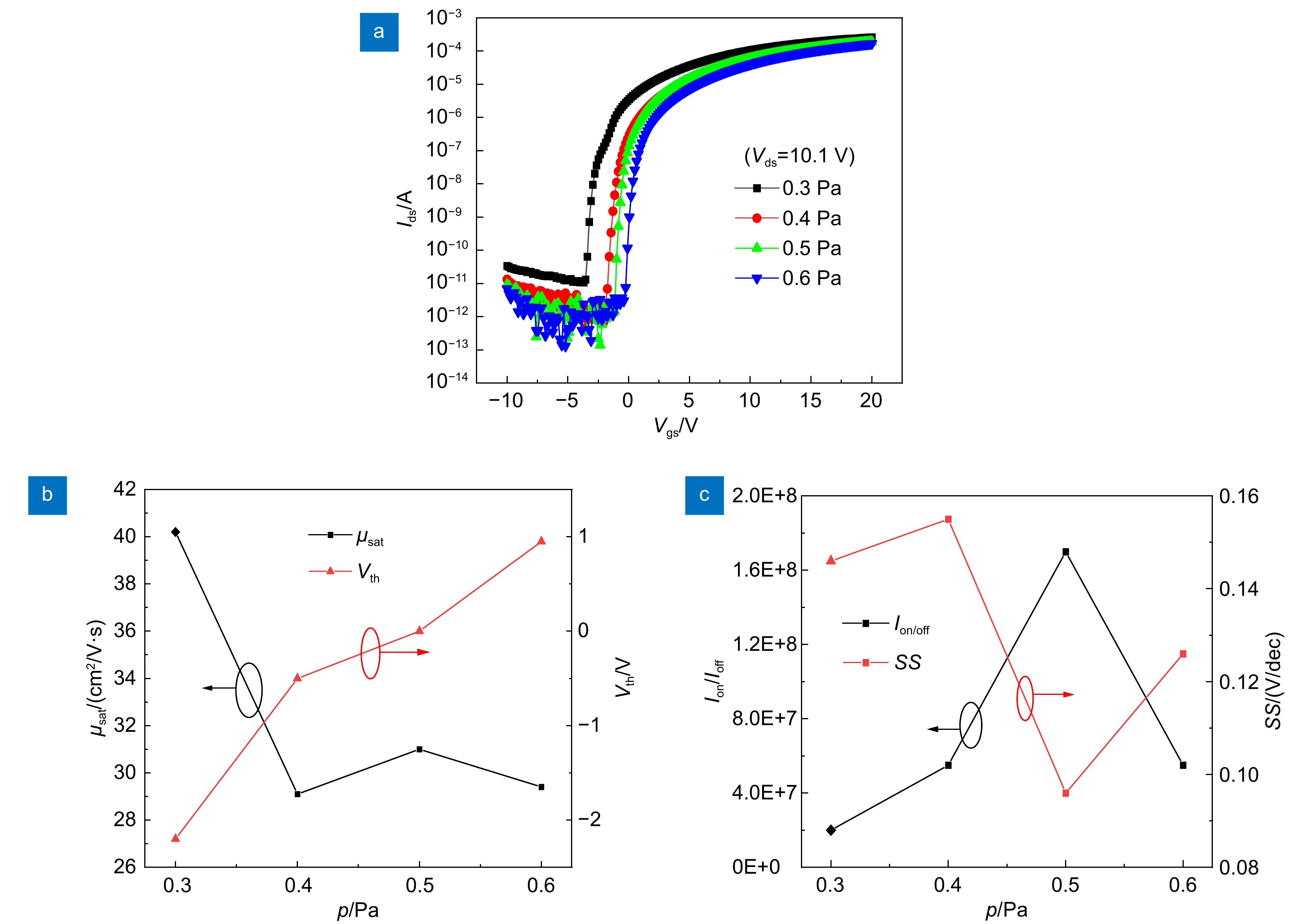
图 5 不同溅射气体压强下制备的IZO TFT电学性能。(a)转移特性;(b) µsat和SS;(c) Vth 和Ion/Ioff
Figure 5. Electrical characteristics of IZO TFT prepared under different sputtering gas pressures. (a) Transfer characteristics; (b) µsat and SS ; (c) Vth and Ion/Ioff
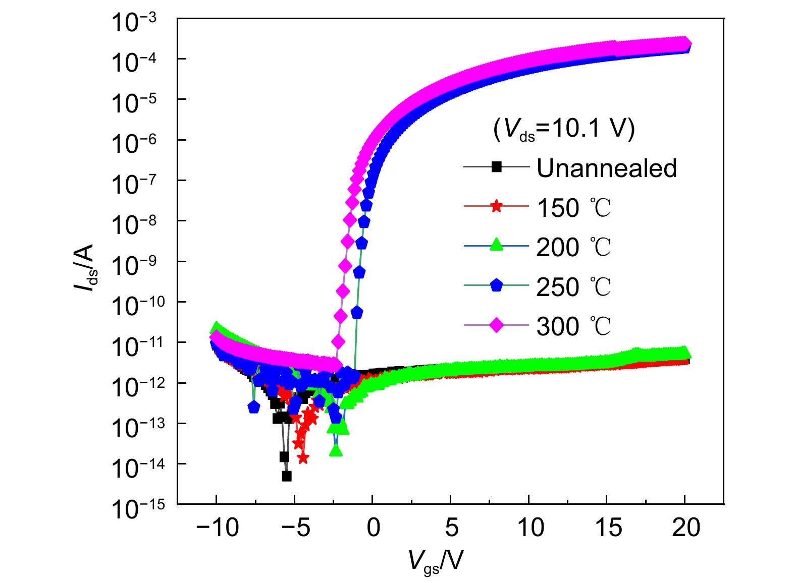
图 6 不同退火温度下IZO TFT的转移特性曲线
Figure 6. Transfer characteristic curves of IZO TFT under different annealing temperatures
-
[1] Lan L F, Xiong N N, Xiao P, et al. Enhancement of bias and illumination stability in thin-film transistors by doping InZnO with wide-band-gap Ta2O5[J]. Appl Phys Lett, 2013, 102(24): 242102. doi: 10.1063/1.4811416
[2] Zhao H L, Tarsoly G, Shan F, et al. Impact of pre-annealing process on electrical properties and stability of indium zinc oxide thin-film transistors[J]. Sci Rep, 2022, 12(1): 19497. doi: 10.1038/s41598-022-24093-w
[3] Li H C, Liu Y R, GENG K W, et al. Temperature dependence of the electrical characteristics of ZnO thin film transistor with high-k NbLaO gate dielectric[J]. J Vac Sci Technol B, 2021, 39(1): 012202. doi: 10.1116/6.0000522
[4] Lu L, Xia Z H, Li J P, et al. A comparative study on fluorination and oxidation of Indium–Gallium–Zinc oxide thin-film transistors[J]. IEEE Electron Device Lett, 2018, 39(2): 196−199. doi: 10.1109/LED.2017.2781700
[5] Seo J S, Jeon J H, Hwang Y H, et al. Solution-processed flexible fluorine-doped indium zinc oxide thin-film transistors fabricated on plastic film at low temperature[J]. Sci Rep, 2013, 3: 2085. doi: 10.1038/srep02085
[6] Heo K J, Tarsoly G, Lee J Y, et al. Improved electrical and temporal stability of In-Zn oxide semiconductor thin-film transistors with organic passivation layer[J]. IEEE J Electron Devices Soc, 2022, 10: 660−665. doi: 10.1109/JEDS.2022.3194921
[7] Park S Y, Song J H, Lee C K, et al. Improvement in photo-bias stability of high-mobility indium zinc oxide thin-film transistors by oxygen high-pressure annealing[J]. IEEE Electron Device Lett, 2013, 34(7): 894−896. doi: 10.1109/LED.2013.2259574
[8] Moon Y K, Lee S, Kim W S, et al. Improvement in the bias stability of amorphous indium gallium zinc oxide thin-film transistors using an O2 plasma-treated insulator[J]. Appl Phys Lett, 2009, 95(1): 013507. doi: 10.1063/1.3167816
[9] Li M, Lan L F, Xu M, et al. Performance improvement of oxide thin-film transistors with a two-step-annealing method[J]. Solid-State Electron, 2014, 91: 9−12. doi: 10.1016/j.sse.2013.09.008
[10] 刘江安. 铟镓锌氧化物与铟锌氧化物靶材的制备及性能研究[D]. 武汉: 华中科技大学, 2021: 89–103.https://doi.org/10.27157/d.cnki.ghzku.2021.006292.
Liu J A. The preparation and study of indium gallium zinc oxide and indium zinc oxide targets[D]. Wuhan: Huazhong University of Science and Technology, 2021: 89–103.https://doi.org/10.27157/d.cnki.ghzku.2021.006292.
[11] 王聪, 刘玉荣. 氧化锌薄膜晶体管电性能的温度特性[J]. 光电工程, 2016, 43(2): 50−54,61. doi: 10.3969/j.issn.1003-501X.2016.02.009
Wang C, Liu Y R. Temperature dependence of the electrical characteristics of ZnO thin film transistors[J]. Opto-Electron Eng, 2016, 43(2): 50−54,61. doi: 10.3969/j.issn.1003-501X.2016.02.009
[12] 王雪霞. a-IGZO TFT制备工艺和性能的研究[D]. 济南: 山东大学, 2014: 35–47.https://doi.org/10.7666/d.Y2595305.
Wang X X. Studies on fabrication processes and properties of a-IGZO TFTs[D]. Jinan: Shandong University, 2014: 35–47.https://doi.org/10.7666/d.Y2595305.
[13] Meyer K, Schuller I K, Falco C M. Thermalization of sputtered atoms[J]. J Appl Phys, 1981, 52(9): 5803−5805. doi: 10.1063/1.329473
[14] Iwamatsu S, Takechi K, Abe Y, et al. Characterization of stress-controlled a-IGZO thin films and their applications to thin-film transistor and micro-electromechanical system processes[C]// 2013 Twentieth International Workshop on Active-Matrix Flatpanel Displays and Devices (AM-FPD), 2013: 133–136.
[15] Alexander M R, Thompson G E, Beamson G. Characterization of the oxide/hydroxide surface of aluminium using x-ray photoelectron spectroscopy: a procedure for curve fitting the O 1s core level[J]. Surf Interface Anal, 2000, 29(7): 468−477. doi: 10.1002/1096-9918(200007)29:7<468::AID-SIA890>3.0.CO;2-V
[16] Hwang S, Lee J H, Woo C H, et al. Effect of annealing temperature on the electrical performances of solution-processed InGaZnO thin film transistors[J]. Thin Solid Films, 2011, 519(15): 5146−5149. doi: 10.1016/j.tsf.2011.01.074
[17] Sung S Y, Jo K M, Kim S Y, et al. Effects of post-annealing treatments on the transfer characteristics of amorphous indium-gallium-zinc oxide thin film transistors[J]. J Nanoelectron Optoelectron, 2011, 6(3): 310−314. doi: 10.1166/jno.2011.1175
-
 下载:
下载:

 点击扫一扫
点击扫一扫
图(7)
计量
- 文章访问数:
- PDF下载数:
- 施引文献: 0


