
 E-mail Alert
 RSS
RSS
-
摘要:
硅基片上功率分束器是光子集成电路的重要组成,具有广泛的应用,比如反馈电路、抽头功率监测和光学量化等。纳米光子器件的设计方法大致可以分为正向设计方法和逆向设计方法。本文概述了正向设计方法和逆向设计方法的区别与联系,并且对逆向设计算法进行了归纳分类,此外,总结了近年来具有代表性的逆向设计的硅基片上功率分束器,包括多通道功率分束器、任意分束比功率分束器、多模式功率分束器、宽带功率分束器和多功能功率分束器,最后对逆向设计算法以及逆向设计的功率分束器的发展趋势进行了总结与展望。
Abstract:The silicon-based on-chip power splitter, an important component of the photonic integrated circuits, has much wider scope of applications such as feedback circuits, tap-port power monitoring, and optical quantization. The design methods of the nanophotonic devices can be roughly divided into the forward design and inverse design methods. This review article outlines the differences and connections between the forward design and inverse design methods, and classifies the inverse design algorithms. In addition, the review article summarizes the representative inverse-designed silicon-based on-chip power splitters in recent years, including multichannel power splitters, arbitrary-split-ratio power splitters, multimode power splitters, broadband power splitters, and multifunction power splitters. Finally, the summary and outlook are made on the development trend of the inverse design algorithms and the inverse-designed power splitters.
-
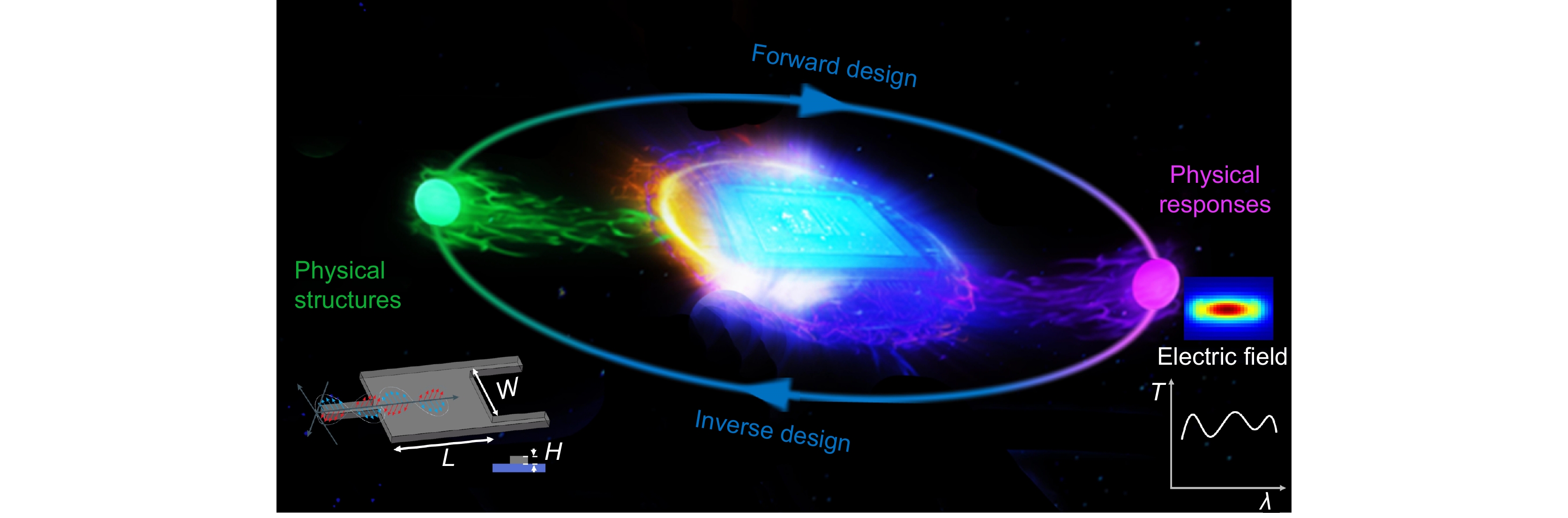
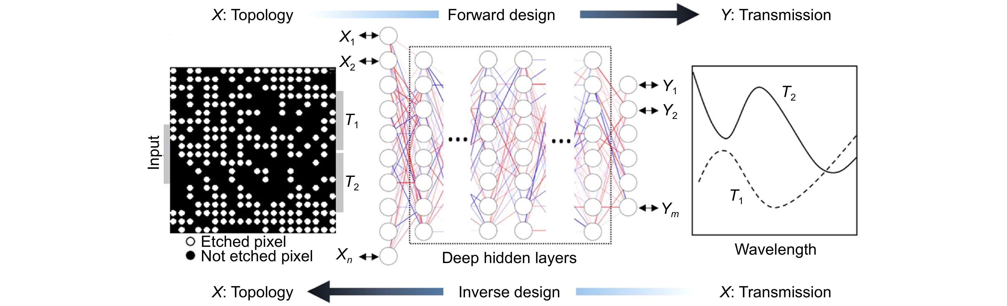
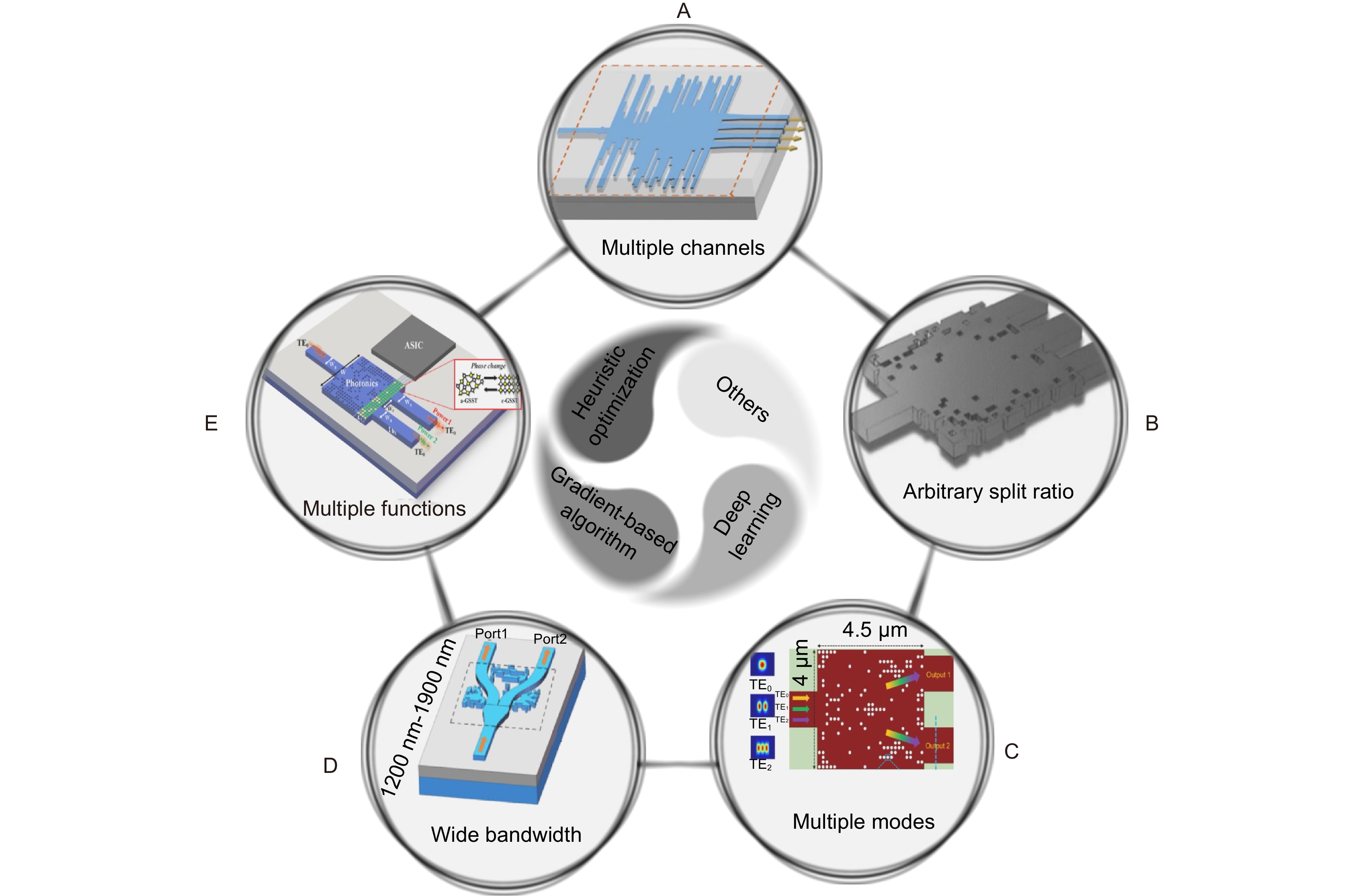
Overview: The photonic integrated circuits (PICs) have been widely accepted as a viable alternative to support futuristic data communication networks. Specifically, silicon photonics offer a more promising and attractive platform to address the growing demands for optical communications due to its unique combination of low fabrication costs, low power consumption, compact footprint, and compatibility with mature complementary metal oxide semiconductor processes. The silicon-based on-chip nanophotonic devices are becoming fundamental building blocks of the complex PICs. The device-design methods can be roughly divided into the forward design and inverse design methods. The forward design method, a mechanism-orientation method, relying on the intuition, experience, and physical effect, usually finds the good device performance by tuning small sets of the characteristic parameters. While remarkable success has been accomplished using the forward design method, the trial-and-error procedure of this method becomes computationally costly and time-inefficient due to the continuously increasing complexity of the nanophotonic devices. In addition, limited by the small parameter search space of the forward-designed nanophotonic device, the device generally occupies a large footprint and has a limited performance. Driven by the increasing demands for the high-density PICs in the practical applications, great progress has been made in the research of the inverse design method. The inverse design method, an objective-orientation method, has been proposed to overcome the shortcomings of the forward design method. The nanophotonic device with the compact footprint and low loss can be designed automatically by the inverse design method. The inverse design method provides a new avenue for the realization of photonic chips. The silicon-based on-chip power splitter has much wider scope of applications such as feedback circuits, tap-port power monitoring, and optical quantization. As a result, the power splitter has been attracting more and more attention in recent years. Although the forward-designed power splitters have good performances, their large footprints limit their further applications in the high-density and large-scale PICs. Inverse-designed silicon-based on-chip power splitters featuring compact footprint, low loss, multiple channels, and flexible functions, has become the key building block for realizing the high-density optical system. In this review, we outline the differences and connections between the forward design and inverse design methods, and classify the inverse design algorithms. In addition, we summarize the representative inverse-designed silicon-based on-chip power splitters in recent years, including multichannel power splitters, arbitrary-split-ratio power splitters, multimode power splitters, broadband power splitters, and multifunction power splitters. Finally, the summary and outlook are made on the development trend of the inverse design algorithms and the inverse-designed power splitters.
-

-

图 1 逆向设计的功率分束器总结。A:4通道的功率分束器[62];B:分束比为1:2:1的功率分束器[63];C:三TE偏振模式的功率分束器[70];D:工作带宽为700 nm功率分束器[71];E:可调谐的功率分束器[72]
Figure 1. Summary of the inverse-designed power splitters. A: The power splitter with four channels [62]; B: The power splitter with a split ratio of 1:2:1 [63]; C: The power splitter for the TE0, TE1, and TE2 modes [70]; D: The power splitter with 700 nm working bandwidth [71]; E: The tunable power splitter [72]
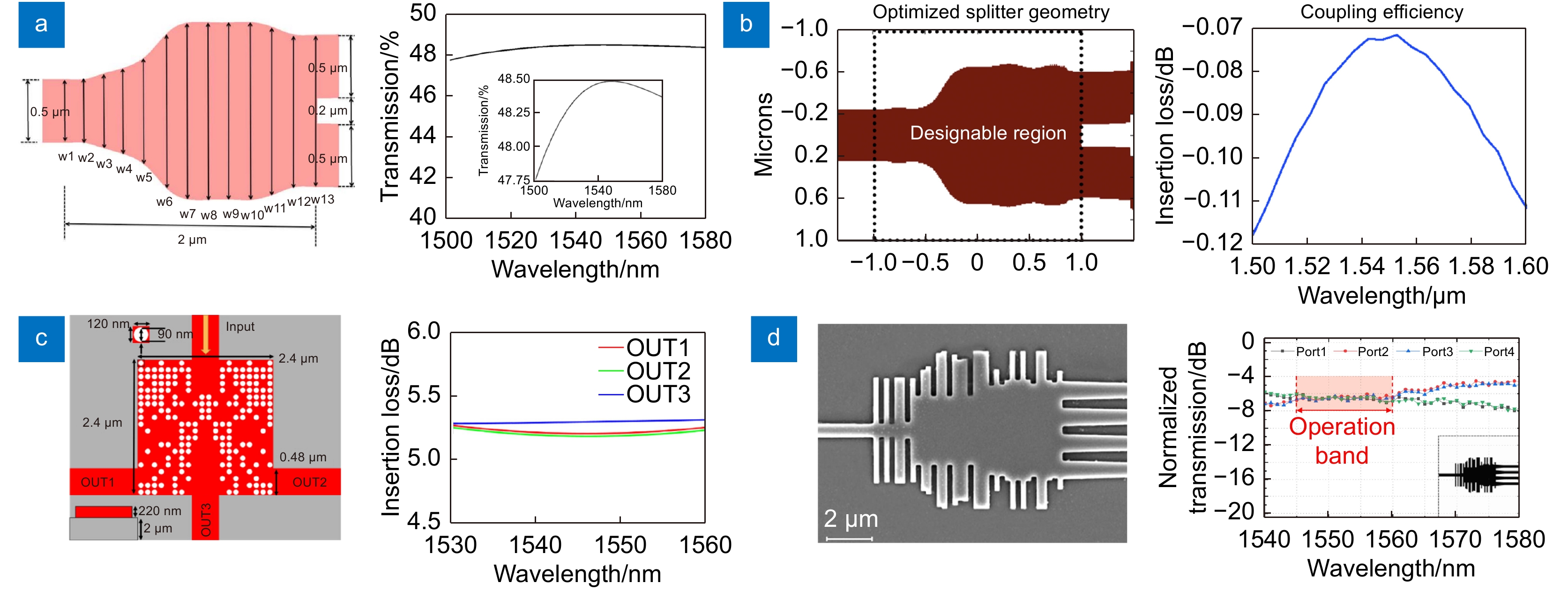
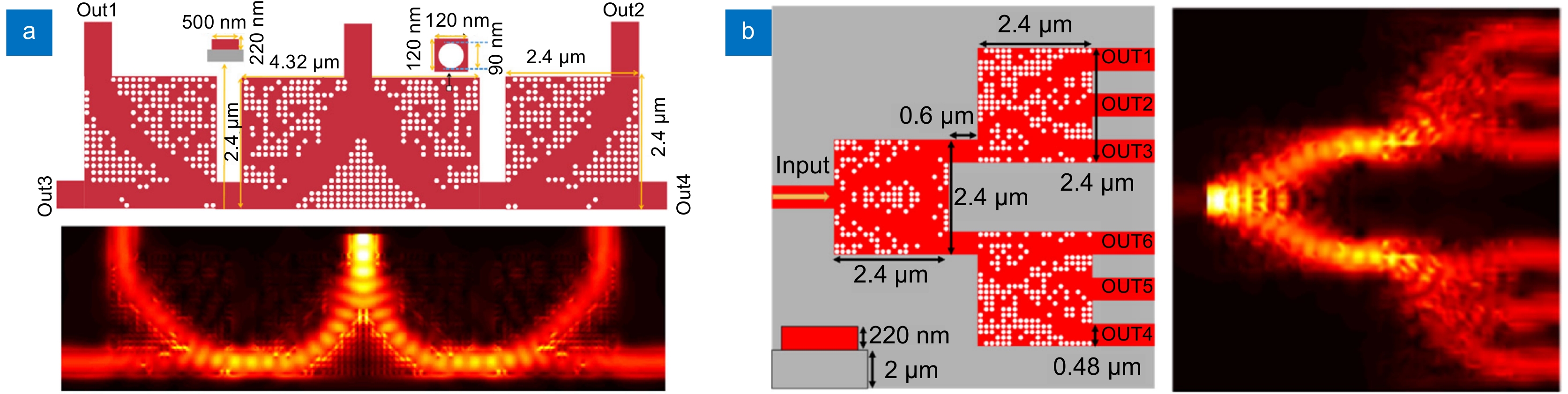
图 4 组合的多通道功率分束器的结构与性能。(a)由三个具有不同输出方向的1×2功率分束器组成的1×4功率分束器[60];(b)由一个1×2功率分束器和两个1×3功率分束器组成的1×6功率分束器[86]
Figure 4. Structures and results of the assembled power splitters with multiple channels. (a) The 1 × 4 power splitter assembled by three 1 × 2 power splitters with different output directions [60]; (b) The 1 × 6 power splitter assembled by one 1 × 2 power splitter and two 1 × 3 power splitters [86]
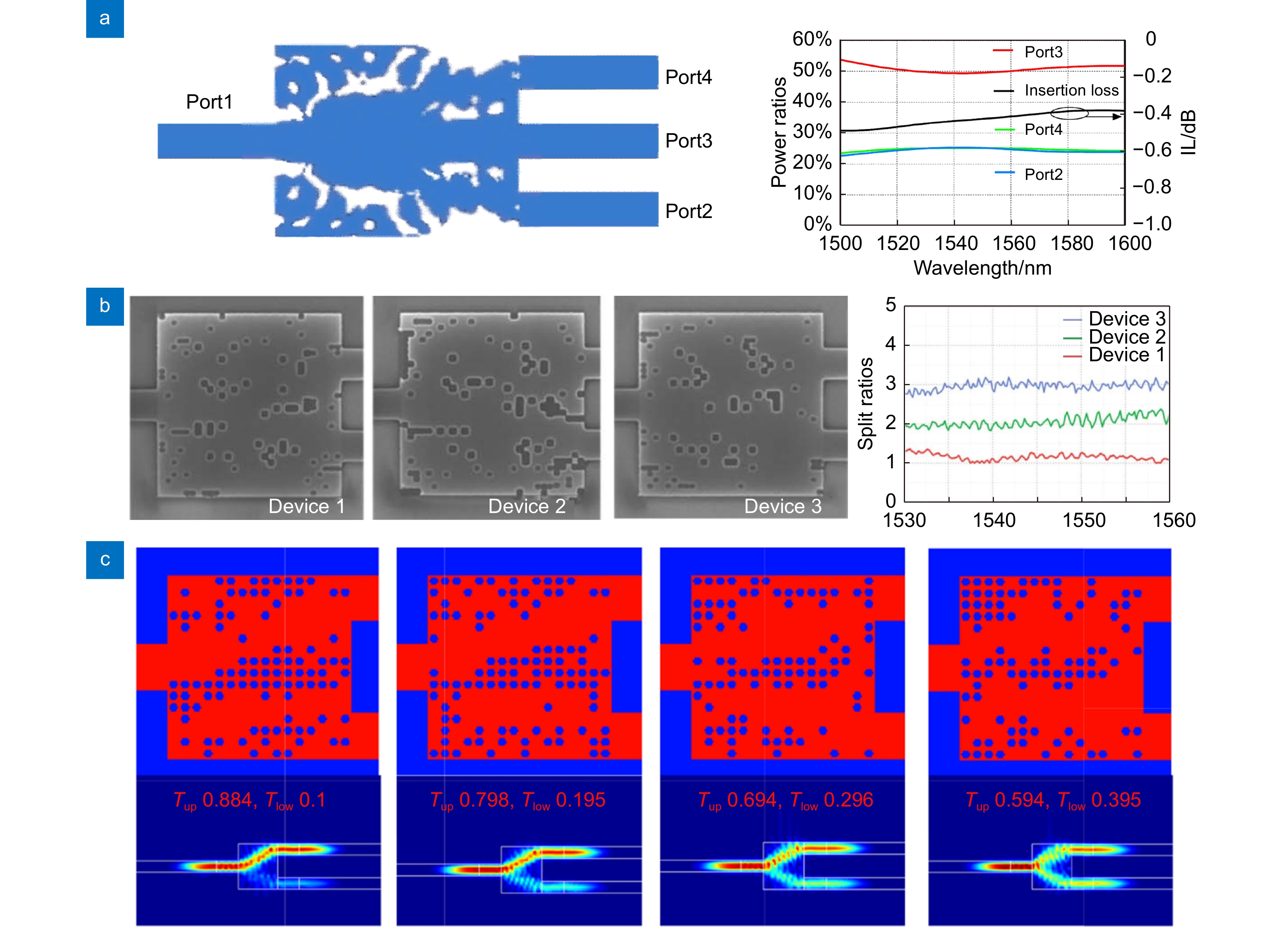
图 5 任意分束比功率分束器的结构和性能。(a)分束比为1:2:1的1×3功率分束器[87];(b)分束比分别为1:1、1:2和1:3的1×2功率分束器[63];(c)分束比分别为9:1、8:2、7:3和6:4的1×2功率分束器[88]
Figure 5. Structures and results of the power splitters with arbitrary split ratios. (a) The 1 × 3 power splitter with a split ratio of 1:2:1 [87]; (b) The 1 × 2 power splitters with the split ratios of 1:1, 1:2, and 1:3 [63]; (c) The 1 × 2 power splitter with the split ratios of 9:1, 8:2, 7:3, and 6:4 [88]
图 7 单个多模式功率分束器的结构和性能。(a)双TE模式功率分束器[90];(b)三TE模式功率分束器[70]; (c)四模式双偏振功率分束器[93]
Figure 7. Structures and results of the single-device power splitters with multiple modes. (a) The two-TE-mode power splitter [90]; (b) The three-TE-mode power splitter [70]; (c) The four-mode and dual-polarization power splitter [93]
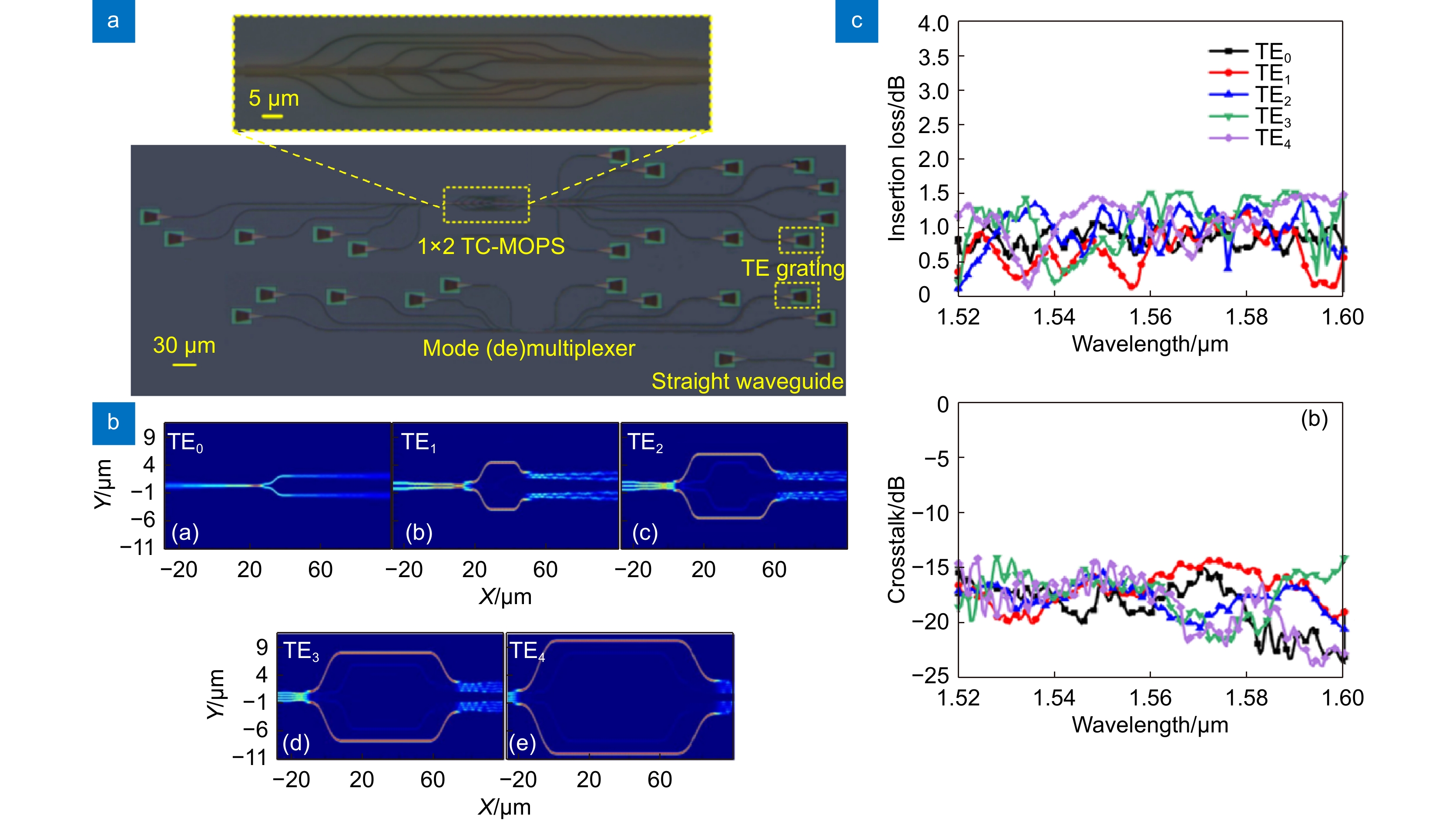
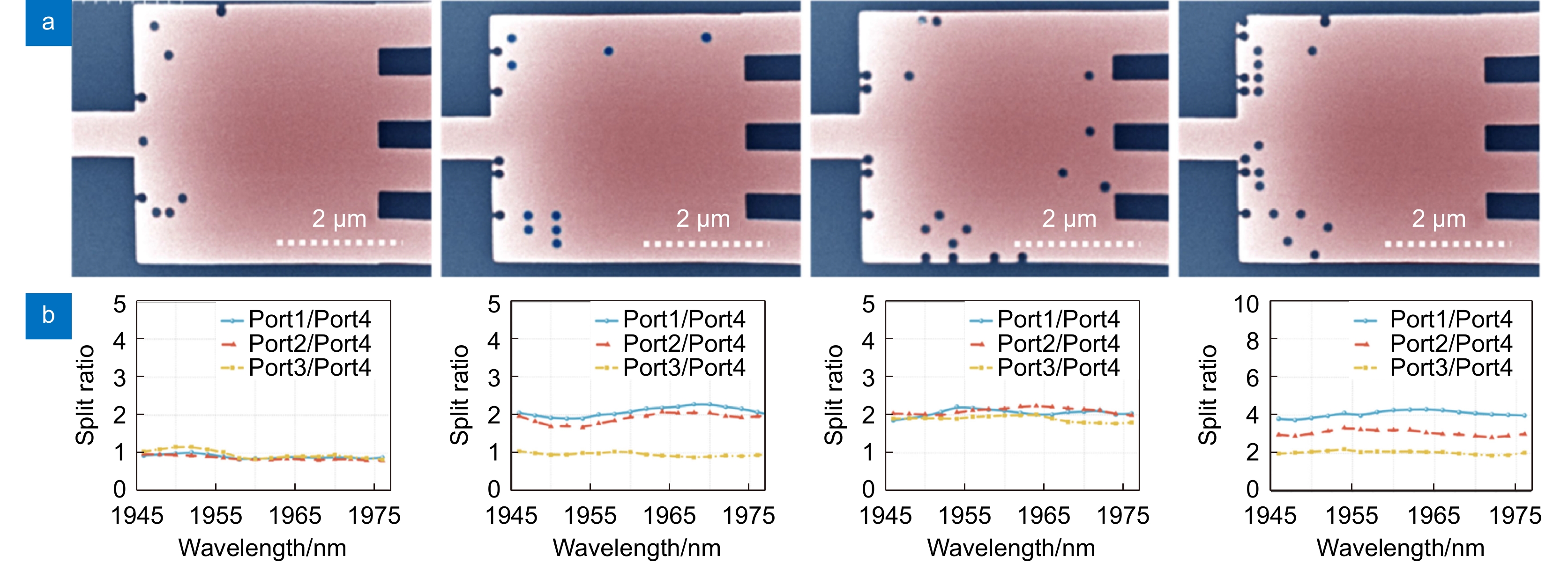
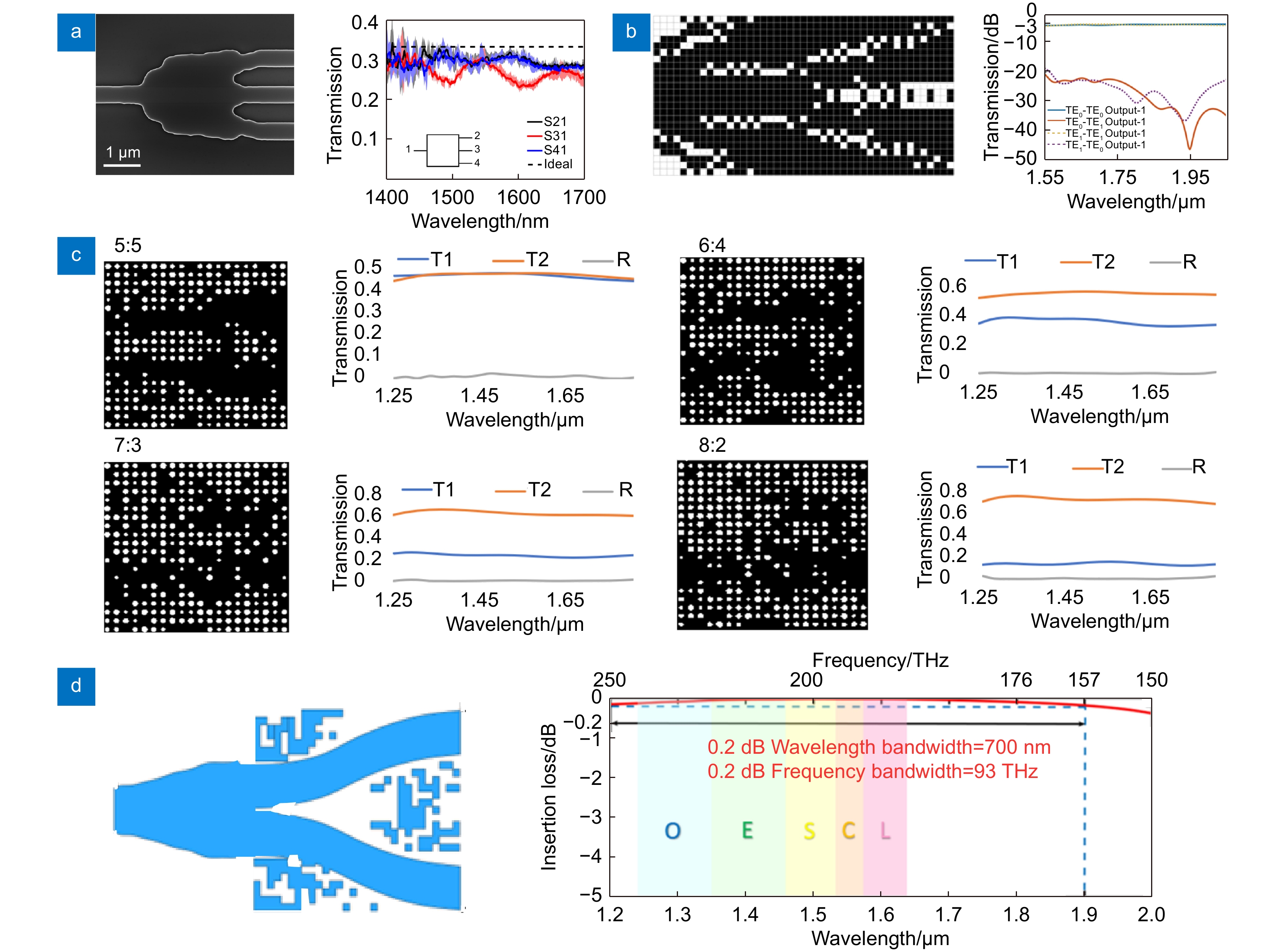
图 10 宽带功率分束器的结构和性能。(a) 300 nm带宽的1×4功率分束器[96];(b) 445 nm带宽的1×2功率分束器[97];(c) 550 nm带宽的1×2功率分束器[98];(d) 700 nm带宽的1×2功率分束器[71]
Figure 10. Structures and results of the broadband power splitters. (a) The 1×4 power splitter with 300 nm working bandwidth [96]; (b) The 1×2 power splitter with 445 nm working bandwidth [97]; (c) The 1×2 power splitter with 550 nm working bandwidth [98]; (d) The 1×2 power splitter with 700 nm working bandwidth [71]
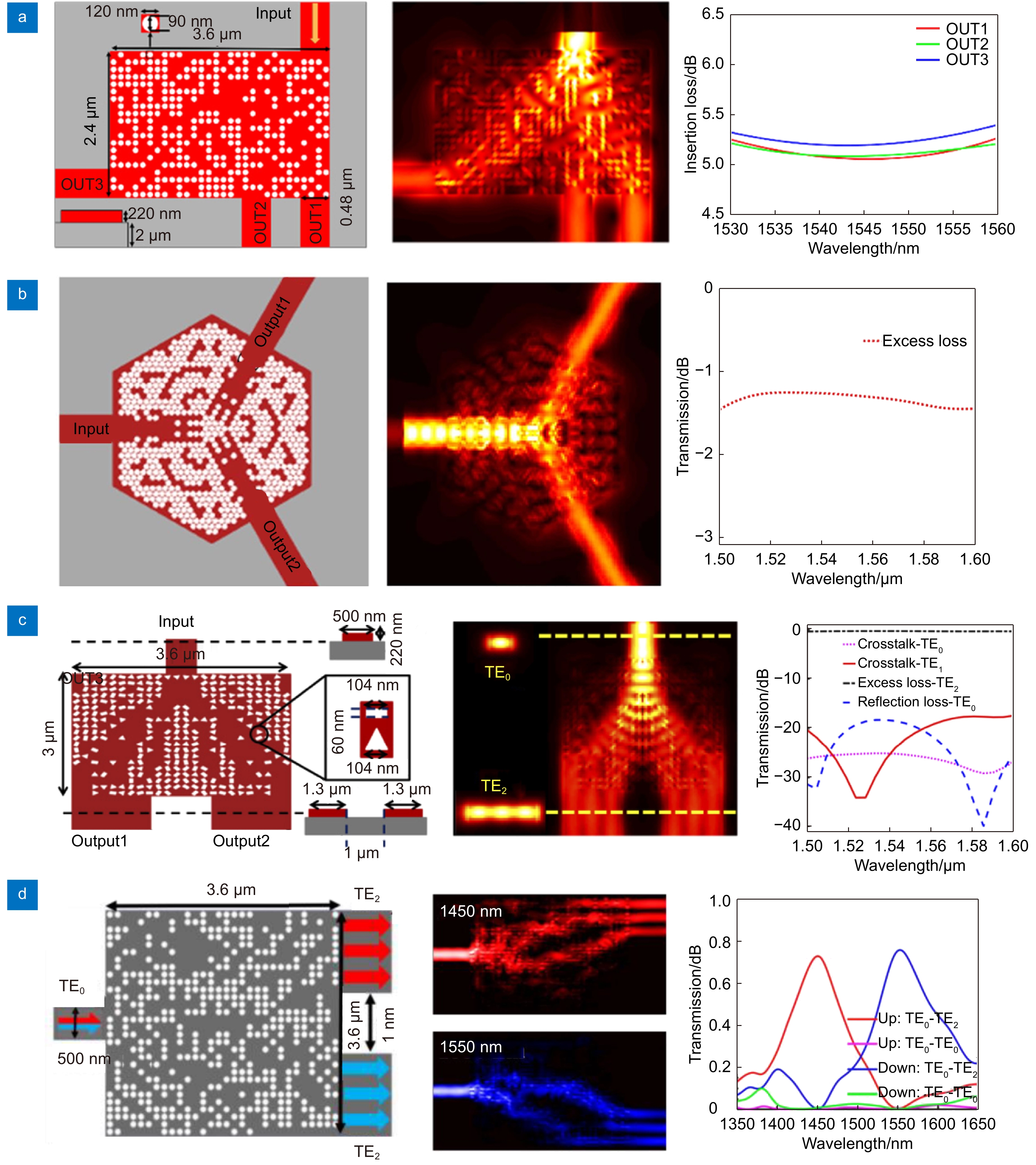
图 11 组合功能功率分束器的结构和性能。(a)具有不同输出方向的功率分束器[86];(b)任意输入的功率分束器[100];(c)模式转换的功率分束器[101];(d)模式转化和波长解复用的功率分束器[102]
Figure 11. Structures and results of the combined-functional power splitters. (a) The power splitter with different output directions [86]; (b) The power splitter with the arbitrary input waveguides [100]; (c) The power splitter with the mode conversion [101]; (d) The power splitter with the mode conversion and wavelength demultiplexing [102]
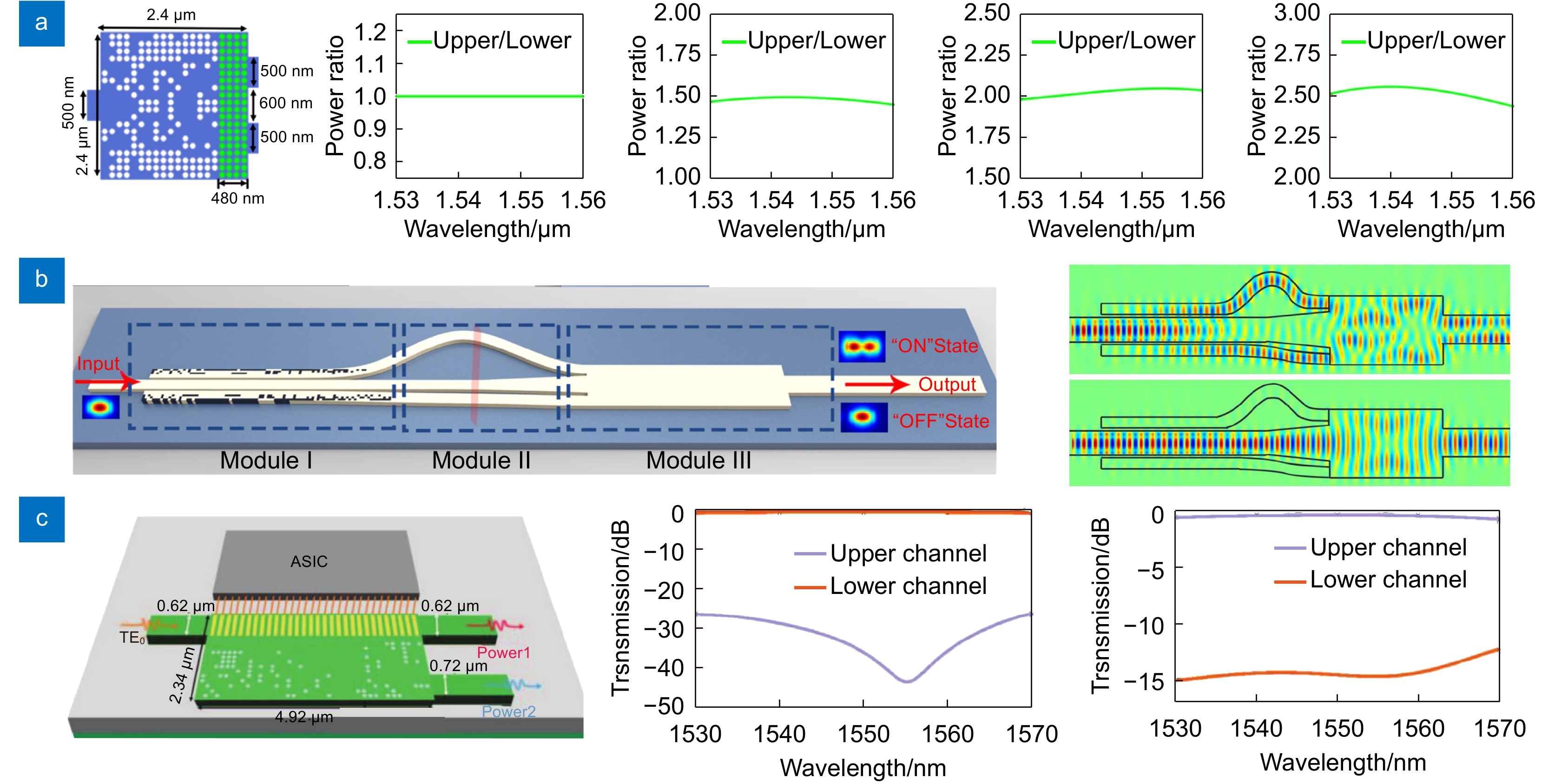
图 12 可调谐功率分束器的结构和性能。(a)基于GSST的可调谐分束比的功率分束器[72];(b)基于GSST的可调谐的直通和分束功能的功率分束器[103];(c)基于Sb2Se3的可调谐分束比的功率分束器[104]
Figure 12. Structures and results of the tunable power splitters. (a) The GST-based power splitter with the reconfigured power ratios [72]; (b) The GSST-based power splitter with the straight passing and power splitting [103]; (c) The Sb2Se3-based power splitter with the reconfigured power ratios [104]
-
[1] Chen Y, Cheng Y K, Zhu R B, et al. Nanoscale all-optical logic devices[J]. Sci China Phys Mech Astron, 2019, 62(4): 44201. doi: 10.1007/s11433-018-9289-3
[2] Reed G T, Mashanovich G, Gardes F Y, et al. Silicon optical modulators[J]. Nat Photonics, 2010, 4(8): 518−526. doi: 10.1038/nphoton.2010.179
[3] Subbaraman H, Xu X C, Hosseini A, et al. Recent advances in silicon-based passive and active optical interconnects[J]. Opt Express, 2015, 23(3): 2487−2511. doi: 10.1364/OE.23.002487
[4] Soref R A, Lorenzo J P. Single-crystal silicon: a new material for 1.3 and 1.6 μm integrated-optical Components[J]. Electron Lett, 1985, 21(21): 953−955. doi: 10.1049/el:19850673
[5] Soref R A, Bennett B R. Electrooptical effects in silicon[J]. IEEE J Quantum Electron, 1987, 23(1): 123−129. doi: 10.1109/JQE.1987.1073206
[6] Soref R A, Bennett B R. Kramers–Kronig analysis of electro-optical switching in silicon[J]. Proc SPIE, 1987, 704: 32−37. doi: 10.1117/12.937193
[7] Hochberg M, Baehr-Jones T. Towards fabless silicon photonics[J]. Nat Photonics, 2010, 4(8): 492−494. doi: 10.1038/nphoton.2010.172
[8] Stojanović V, Ram R J, Popović M, et al. Monolithic silicon-photonic platforms in state-of-the-art CMOS SOI processes [Invited][J]. Opt Express, 2018, 26(10): 13106. doi: 10.1364/OE.26.013106
[9] Dong P, Chen Y K, Duan G H, et al. Silicon photonic devices and integrated circuits[J]. Nanophotonics, 2014, 3(4–5): 215−228. doi: 10.1515/nanoph-2013-0023
[10] Zalevsky Z. Integrated micro- and nanophotonic dynamic devices: a review[J]. J Nanophoton, 2007, 1(1): 012504. doi: 10.1117/1.2795715
[11] Wang J, Long Y. On-chip silicon photonic signaling and processing: a review[J]. Sci Bull, 2018, 63(19): 1267−1310. doi: 10.1016/j.scib.2018.05.038
[12] Xu Q F, Fattal D, Beausoleil R G. Silicon microring resonators with 1.5-μm radius[J]. Opt Express, 2008, 16(6): 4309−4315. doi: 10.1364/OE.16.004309
[13] Chen P X, Chen S T, Guan X W, et al. High-order microring resonators with bent couplers for a box-like filter response[J]. Opt Lett, 2014, 39(21): 6304−6307. doi: 10.1364/OL.39.006304
[14] Stern B, Zhu X L, Chen C P, et al. On-chip mode-division multiplexing switch[J]. Optica, 2015, 2(6): 530−535. doi: 10.1364/OPTICA.2.000530
[15] Xu Q F, Schmidt B, Pradhan S, et al. Micrometre-scale silicon electro-optic modulator[J]. Nature, 2005, 435(19): 325−327. doi: 10.1038/nature03569
[16] Bogaerts W, De Heyn P, van Vaerenbergh T, et al. Silicon microring resonators[J]. Laser Photonics Rev, 2012, 6(1): 47−73. doi: 10.1002/lpor.201100017
[17] Ji Y, Chung Y, Sprinzak D, et al. An electronic Mach-Zehnder interferometer[J]. Nature, 2003, 422(6930): 415−418. doi: 10.1038/nature01503
[18] Shen Y C, Harris N C, Skirlo S, et al. Deep learning with coherent nanophotonic circuits[J]. Nat Photonics, 2017, 11(7): 441−446. doi: 10.1038/nphoton.2017.93
[19] Harris N C, Steinbrecher G R, Prabhu M, et al. Quantum transport simulations in a programmable nanophotonic processor[J]. Nat Photonics, 2017, 11(7): 447−452. doi: 10.1038/nphoton.2017.95
[20] Pérez D, Gasulla I, Crudgington L, et al. Multipurpose silicon photonics signal processor core[J]. Nat Commun, 2017, 8(1): 636. doi: 10.1038/s41467-017-00714-1
[21] Xie Y W, Hong S H, Yan H, et al. Low-loss chip-scale programmable silicon photonic processor[J]. Opto-Electron Adv, 2023, 6(3): 220030. doi: 10.29026/oea.2023.220030
[22] Xiao Z, Luo X S, Lim P H, et al. Ultra-compact low loss polarization insensitive silicon waveguide splitter[J]. Opt Express, 2013, 21(14): 16331−16336. doi: 10.1364/OE.21.016331
[23] Uematsu T, Ishizaka Y, Kawaguchi Y, et al. Design of a compact two-mode multi/demultiplexer consisting of multimode interference waveguides and a wavelength-insensitive phase shifter for mode-division multiplexing transmission[J]. J Lightwave Technol, 2012, 30(15): 2421−2426. doi: 10.1109/JLT.2012.2199961
[24] Li Y M, Li C, Li C B, et al. Compact two-mode (de) multiplexer based on symmetric Y-junction and multimode interference waveguides[J]. Opt Express, 2014, 22(5): 5781−5786. doi: 10.1364/OE.22.005781
[25] Han L S, Liang S, Zhu H L, et al. Two-mode de/multiplexer based on multimode interference couplers with a tilted joint as phase shifter[J]. Opt Lett, 2015, 40(4): 518−521. doi: 10.1364/OL.40.000518
[26] Li C L, Liu D J, Dai D X. Multimode silicon photonics[J]. Nanophotonics, 2019, 8(2): 227−247. doi: 10.1515/nanoph-2018-0161
[27] Ding Y H, Xu J, Da Ros F, et al. On-chip two-mode division multiplexing using tapered directional coupler-based mode multiplexer and demultiplexer[J]. Opt Express, 2013, 21(8): 10376−10382. doi: 10.1364/OE.21.010376
[28] Mohammed Z, Paredes B, Rasras M. Compact and broadband silicon TE-pass polarizer based on tapered directional coupler[J]. Opt Lett, 2022, 47(14): 3399−3402. doi: 10.1364/OL.457260
[29] Wang J, He S L, Dai D X. On-chip silicon 8-channel hybrid (de)multiplexer enabling simultaneous mode- and polarization-division-multiplexing[J]. Laser Photonics Rev, 2014, 8(2): L18−L22. doi: 10.1002/lpor.201300157
[30] Dai D X, Li C L, Wang S P, et al. 10-channel mode (de)multiplexer with dual polarizations[J]. Laser Photonics Rev, 2018, 12(1): 1700109. doi: 10.1002/lpor.201700109
[31] Greenberg M, Orenstein M. Multimode add-drop multiplexing by adiabatic linearly tapered coupling[J]. Opt Express, 2005, 13(23): 9381−9387. doi: 10.1364/OPEX.13.009381
[32] Dai D X, Bowers J E. Novel concept for ultracompact polarization splitter-rotator based on silicon nanowires[J]. Opt Express, 2011, 19(11): 10940−10949. doi: 10.1364/OE.19.010940
[33] Dai D X, Wu H. Realization of a compact polarization splitter-rotator on silicon[J]. Opt Lett, 2016, 41(10): 2346−2349. doi: 10.1364/OL.41.002346
[34] Sacher W D, Barwicz T, Taylor B J F, et al. Polarization rotator-splitters in standard active silicon photonics platforms[J]. Opt Express, 2014, 22(4): 3777−3786. doi: 10.1364/OE.22.003777
[35] Huang J, Ma H S, Chen D B, et al. Digital nanophotonics: the highway to the integration of subwavelength-scale photonics: ultra-compact, multi-function nanophotonic design based on computational inverse design[J]. Nanophotonics, 2021, 10(3): 1011−1030. doi: 10.1515/NANOPH-2020-0494
[36] Lu J, Vučković J. Nanophotonic computational design[J]. Opt Express, 2013, 21(11): 13351−13367. doi: 10.1364/OE.21.013351
[37] Yao K, Unni R, Zheng Y B. Intelligent nanophotonics: merging photonics and artificial intelligence at the nanoscale[J]. Nanophotonics, 2019, 8(3): 339−366. doi: 10.1515/nanoph-2018-0183
[38] Ma L F, Li J, Liu Z H, et al. Intelligent algorithms: new avenues for designing nanophotonic devices[J]. Chin Opt Lett, 2021, 19(1): 011301. doi: 10.3788/COL202119.011301
[39] Qi H X, Du Z C, Hu X Y, et al. High performance integrated photonic circuit based on inverse design method[J]. Opto-Electron Adv, 2022, 5(10): 210061. doi: 10.29026/oea.2022.210061
[40] Jiang J Q, Chen M K, Fan J A. Deep neural networks for the evaluation and design of photonic devices[J]. Nat Rev Mater, 2021, 6(8): 679−700. doi: 10.1038/s41578-020-00260-1
[41] So S, Badloe T, Noh J, et al. Deep learning enabled inverse design in nanophotonics[J]. Nanophotonics, 2020, 9(5): 1041−1057. doi: 10.1515/nanoph-2019-0474
[42] Ma T G, Tobah M, Wang H Z, et al. Benchmarking deep learning-based models on nanophotonic inverse design problems[J]. Opto-Electron Sci, 2022, 1(1): 210012. doi: 10.29026/oes.2022.210012
[43] Wang N, Yan W, Qu Y R, et al. Intelligent designs in nanophotonics: from optimization towards inverse creation[J]. PhotoniX, 2021, 2(1): 22. doi: 10.1186/s43074-021-00044-y
[44] Huang J, Yang J B, Chen D B, et al. Implementation of on-chip multi-channel focusing wavelength demultiplexer with regularized digital metamaterials[J]. Nanophotonics, 2020, 9(1): 159−166. doi: 10.1515/nanoph-2019-0368
[45] Liu Z H, Liu X H, Xiao Z Y, et al. Integrated nanophotonic wavelength router based on an intelligent algorithm[J]. Optica, 2019, 6(10): 1367−1373. doi: 10.1364/OPTICA.6.001367
[46] Khoram E, Qian X P, Yuan M, et al. Controlling the minimal feature sizes in adjoint optimization of nanophotonic devices using b-spline surfaces[J]. Opt Express, 2020, 28(5): 7060−7069. doi: 10.1364/OE.384438
[47] Han J M, Huang J, Wu J G, et al. Inverse designed tunable four-channel wavelength demultiplexer[J]. Opt Commun, 2020, 465: 125606. doi: 10.1016/j.optcom.2020.125606
[48] Shen B, Wang P, Polson R, et al. An integrated-nanophotonics polarization beamsplitter with 2.4 × 2.4 μm2 footprint[J]. Nat Photonics, 2017, 9(6): 378−382. doi: 10.1038/nphoton.2015.80
[49] Chang W J, Xu S Y, Cheng M F, et al. Inverse design of a single-step-etched ultracompact silicon polarization rotator[J]. Opt Express, 2020, 28(19): 28343−28351. doi: 10.1364/OE.399052
[50] Ma H S, Du T, Zhang Z J, et al. Inverse design of an air-cladding and fully-etched silicon polarization rotator based on a taper-based mode hybridization[J]. Opt Commun, 2023, 526: 128912. doi: 10.1016/j.optcom.2022.128912
[51] Lu C C, Liu Z H, Wu Y, et al. Nanophotonic polarization routers based on an intelligent algorithm[J]. Adv Opt Mater, 2020, 8(10): 1902018. doi: 10.1002/adom.201902018
[52] Ma H S, Luo M Y, He J, et al. Inverse design of nonvolatile reconfigurable mode generator and optical circulator based on a novel concept of a fully-digitized module[J]. J Lightwave Technol, 2022, 40(24): 7869−7878. doi: 10.1109/JLT.2022.3206430
[53] Ren Y M, Zhang L X, Wang W Q, et al. Genetic-algorithm-based deep neural networks for highly efficient photonic device design[J]. Photonics Res, 2021, 9(6): B247−B252. doi: 10.1364/PRJ.416294
[54] Zhou H L, Wang Y L, Gao X Y, et al. Dielectric metasurfaces enabled ultradensely integrated multidimensional optical system[J]. Laser Photonics Rev, 2022, 16(4): 2100521. doi: 10.1002/LPOR.202100521
[55] Xie H C, Liu Y J, Wang S, et al. Highly compact and efficient four-mode multiplexer based on pixelated waveguides[J]. IEEE Photonics Technol Lett, 2020, 32(3): 166−169. doi: 10.1109/LPT.2020.2964308
[56] Han H L, Li H, Zhang X P, et al. High performance ultra-compact SOI waveguide crossing[J]. Opt Express, 2018, 26(20): 25602−25610. doi: 10.1364/OE.26.025602
[57] Lu L L Z, Zhang M M, Zhou F Y, et al. Inverse-designed ultra-compact star-crossings based on PhC-like subwavelength structures for optical intercross connect[J]. Opt Express, 2017, 25(15): 18355−18364. doi: 10.1364/OE.25.018355
[58] Liu Y J, Xu K, Wang S, et al. Arbitrarily routed mode-division multiplexed photonic circuits for dense integration[J]. Nature Communications, 2019, 10(1): 3263. doi: 10.1038/s41467-019-11196-8
[59] Chang W J, Lu L L Z, Ren X S, et al. Ultracompact dual-mode waveguide crossing based on subwavelength multimode-interference couplers[J]. Photonics Res, 2018, 6(7): 660−665. doi: 10.1364/PRJ.6.000660
[60] Ma H S, Huang J, Zhang K W, et al. Arbitrary-direction, multichannel and ultra-compact power splitters by inverse design method[J]. Opt Commun, 2020, 462: 125329. doi: 10.1016/j.optcom.2020.125329
[61] Lu L, Liu D M, Zhou F Y, et al. Inverse-designed single-step-etched colorless 3 dB couplers based on RIE-lag-insensitive PhC-like subwavelength structures[J]. Opt Lett, 2016, 41(21): 5051−5054. doi: 10.1364/OL.41.005051
[62] Kim J, Kim J Y, Yoon J, et al. Experimental demonstration of inverse-designed silicon integrated photonic power splitters[J]. Nanophotonics, 2022, 11(20): 4581−4590. doi: 10.1515/nanoph-2022-0443
[63] Xu K, Liu L, Wen X, et al. Integrated photonic power divider with arbitrary power ratios[J]. Opt Lett, 2017, 42(4): 855−858. doi: 10.1364/OL.42.000855
[64] Gamet J, Pandraud G. Ultralow-loss 1 X 8 splitter based on field matching Y junction[J]. IEEE Photonics Technol Lett, 2004, 16(9): 2060−2062. doi: 10.1109/LPT.2004.833071
[65] Tao S H, Fang Q, Song J F, et al. Cascade wide-angle Y-junction 1 × 16 optical power splitter based on silicon wire waveguides on silicon-on-insulator[J]. Opt Express, 2008, 16(26): 21456−21461. doi: 10.1364/OE.16.021456
[66] Luo Y C, Yu Y, Ye M Y, et al. Integrated dual-mode 3 dB power coupler based on tapered directional coupler[J]. Sci Rep, 2016, 6: 23516. doi: 10.1038/srep23516
[67] Huang W P. Coupled-mode theory for optical waveguides: an overview[J]. J Opt Soc Am A-Opt Image Sci Vis, 1994, 11(3): 963−983. doi: 10.1364/JOSAA.11.000963
[68] Yao R K, Li H X, Zhang B H, et al. Compact and low-insertion-loss 1×N power splitter in silicon photonics[J]. J Lightwave Technol, 2021, 39(19): 6253−6259. doi: 10.1109/JLT.2021.3098346
[69] Sheng Z, Wang Z Q, Qiu C, et al. A compact and low-Loss MMI coupler fabricated with CMOS technology[J]. IEEE Photonics J, 2012, 4(6): 2272−2277. doi: 10.1109/JPHOT.2012.2230320
[70] Xie H C, Liu Y J, Wang Y H, et al. An ultra-compact 3-dB power splitter for three modes based on pixelated meta-structure[J]. IEEE Photonics Technol Lett, 2020, 32(6): 341−344. doi: 10.1109/LPT.2020.2975128
[71] Wang Z C, Peng Z, Zhang Y Q, et al. 93-THz ultra-broadband and ultra-low loss Y-junction photonic power splitter with phased inverse design[J]. Opt Express, 2023, 31(10): 15904−15916. doi: 10.1364/OE.489550
[72] Yuan H, Wu J G, Zhang J P, et al. Non-volatile programmable ultra-small photonic arbitrary power splitters[J]. Nanomaterials, 2022, 12(4): 669. doi: 10.3390/nano12040669
[73] Jiang X P, Yuan H, Chen D B, et al. Metasurface based on inverse design for maximizing solar spectral absorption[J]. Adv Opt Mater, 2021, 9(19): 2100575. doi: 10.1002/adom.202100575
[74] Yu Z J, Cui H R, Sun X K. Genetically optimized on-chip wideband ultracompact reflectors and Fabry–Perot cavities[J]. Photonics Res, 2017, 5(6): B15−B19. doi: 10.1364/PRJ.5.000B15
[75] Zhang Y, Yang S Y, Lim A E J, et al. A compact and low loss Y-junction for submicron silicon waveguide[J]. Opt Express, 2013, 21(1): 1310. doi: 10.1364/OE.21.001310
[76] Goudarzi K, Lee M. Inverse design of a binary waveguide crossing by the particle swarm optimization algorithm[J]. Results Phys, 2022, 34: 105268. doi: 10.1016/j.rinp.2022.105268
[77] Liang W, Chen W W, Wang P J, et al. Non-volatile polarization-insensitive 1 × 2 silicon optical switch using phase-change materials[J]. Opt Commun, 2021, 479: 126407. doi: 10.1016/j.optcom.2020.126407
[78] Peng Z, Feng J B, Du T, et al. Series of ultra-low loss and ultra-compact multichannel silicon waveguide crossing[J]. Opt Express, 2022, 30(15): 27366−27380. doi: 10.1364/OE.462479
[79] Lalau-Keraly C M, Bhargava S, Miller O D, et al. Adjoint shape optimization applied to electromagnetic design[J]. Opt Express, 2013, 21(18): 21693−21701. doi: 10.1364/OE.21.021693
[80] Wang K Y, Ren X S, Chang W J, et al. Inverse design of digital nanophotonic devices using the adjoint method[J]. Photonics Res, 2020, 8(4): 528−533. doi: 10.1364/PRJ.383887
[81] Huang J, Yang J B, Chen D B, et al. Ultra-compact broadband polarization beam splitter with strong expansibility[J]. Photonics Res, 2018, 6(6): 574−578. doi: 10.1364/PRJ.6.000574
[82] Michaels A, Yablonovitch E. Leveraging continuous material averaging for inverse electromagnetic design[J]. Opt Express, 2018, 26(24): 31717−31737. doi: 10.1364/OE.26.031717
[83] Lebbe N, Glière A, Hassan K. High-efficiency and broadband photonic polarization rotator based on multilevel shape optimization[J]. Opt Lett, 2019, 44(8): 1960−1963. doi: 10.1364/OL.44.001960
[84] Bendsøe M P, Kikuchi N. Generating optimal topologies in structural design using a homogenization method[J]. Comput Methods Appl Mech Eng, 1988, 71(2): 197−224. doi: 10.1016/0045-7825(88)90086-2
[85] Wu C M, Yu H S, Lee S, et al. Programmable phase-change metasurfaces on waveguides for multimode photonic convolutional neural network[J]. Nat Commun, 2021, 12(1): 96. doi: 10.1038/s41467-020-20365-z
[86] Xu Y H, Ma H S, Xie T, et al. Ultra-compact power splitters with low loss in arbitrary direction based on inverse design method[J]. Photonics, 2021, 8(11): 516. doi: 10.3390/photonics8110516
[87] Meng C, Qiu J F, Tian Y, et al. A broadband compact 1×3 power splitter designed with inverse design method[C]//Proceedings of the 15th International Conference on Optical Communications and Networks (ICOCN), 2016. https://doi.org/10.1109/icocn.2016.7875589.
[88] Fujisawa T, Saitoh K. Bayesian direct-binary-search algorithm for the efficient design of mosaic-based power splitters[J]. OSA Continuum, 2021, 4(4): 1258−1270. doi: 10.1364/OSAC.422116
[89] Tahersima M H, Kojima K, Koike-Akino T, et al. Deep neural network inverse design of integrated photonic power splitters[J]. Sci Rep, 2019, 9(1): 1368. doi: 10.1038/s41598-018-37952-2
[90] Chang W J, Lu L L Z, Liu D M, et al. An ultra-compact colorless dual-mode 3 dB power splitter based on axisymmetrical subwavelength structure[C]//CLEO: Science and Innovations 2018, 2018: JW2A. 47. https://doi.org/10.1364/CLEO_AT.2018.JW2A.47.
[91] Guo Z Z, Xiao J B. Silicon-based Ultracompact TE-Pass/TM-Stop power divider using subwavelength gratings assisted with segmented hybrid plasmonic horizontal slot waveguides[J]. J Lightwave Technol, 2017, 35(19): 4329−4336. doi: 10.1109/JLT.2017.2740975
[92] Chen Y F, Zhang J, Zhu M, et al. Ultra-compact and broadband all-silicon TM-pass power splitter using subwavelength holey-structured metamaterial waveguides[J]. Opt Express, 2022, 30(25): 44604−44616. doi: 10.1364/OE.477109
[93] Liu Y J, Wang Z, Liu Y L, et al. Ultra-compact mode-division multiplexed photonic integrated circuit for dual polarizations[J]. J Lightwave Technol, 2021, 39(18): 5925−5932. doi: 10.1109/JLT.2021.3092941
[94] Chen W W, Lin J, Li H X, et al. Broadband multimode 3 dB optical power splitter using tapered couplers[J]. Optics Express, 2022, 30(26): 46236−46247. doi: 10.1364/OE.471397
[95] Xie H C, Liu Y J, Sun W Z, et al. Inversely designed 1×4 power splitter with arbitrary ratios at 2-μm spectral band[J]. IEEE Photonics J, 2018, 10(4): 2700506. doi: 10.1109/jphot.2018.2863122
[96] Piggott A Y, Petykiewicz J, Su L, et al. Fabrication-constrained inverse design of a broadband 3-way power splitter[Z]. arXiv: 1612.03222, 2017. https://doi.org/10.48550/arXiv.1612.03222.
[97] Xu J F, Liu Y J, Guo X Y, et al. Inverse design of a dual-mode 3-dB optical power splitter with a 445 nm bandwidth[J]. Opt Express, 2022, 30(15): 26266−26274. doi: 10.1364/OE.463274
[98] Tang Y H, Kojima K, Koike-Akino T, et al. Generative deep learning model for a multi-level Nano-optic broadband power splitter[C]// 2020 Optical Fiber Communications Conference and Exhibition (OFC), 2020: Th1A. 1. https://doi.org/10.1364/OFC.2020.Th1A.1.
[99] Piggott A Y, Lu J, Babinec T M, et al. Inverse design and implementation of a wavelength demultiplexing grating coupler[J]. Sci Rep, 2015, 4: 7210. doi: 10.1038/srep07210
[100] Ma H S, Huang J, Zhang K W, et al. Inverse-designed arbitrary-input and ultra-compact 1 × N power splitters based on high symmetric structure[J]. Sci Rep, 2020, 10: 11757. doi: 10.1038/s41598-020-68746-0
[101] Ma H S, Huang J, Yang J B, et al. Ultra-compact and efficient 1 × 2 mode converters based on rotatable direct-binary-search algorithm[J]. Opt Express, 2020, 28(11): 17010−17019. doi: 10.1364/OE.392145
[102] Yuan H, Huang J, Wang Z H, et al. An ultra-compact dual-channel multimode wavelength demultiplexer based on inverse design[J]. Results Phys, 2021, 27: 104489. doi: 10.1016/j.rinp.2021.104489
[103] Chen H X, Jia H, Wang T, et al. Broadband nonvolatile tunable mode-order converter based on silicon and optical phase change materials hybrid meta-structure[J]. J Lightwave Technol, 2020, 38(7): 1874−1879. doi: 10.1109/JLT.2020.2968565
[104] Yuan H, Wang Z C, Peng Z, et al. Ultra-compact and nonvolatile nanophotonic neural networks[J]. Adv Opt Mater, 2023. doi: 10.1002/adom.202300215
[105] Su Y X, Liu D M, Zhang M M. Sb2Se3-assisted reconfigurable broadband Y-junction[J]. Opt Express, 2022, 30(22): 40379−40388. doi: 10.1364/OE.473157
[106] Chang W J, Lu L L Z, Ren X S, et al. Ultra-compact mode (de) multiplexer based on subwavelength asymmetric Y-junction[J]. Opt Express, 2018, 26(7): 8162−8170. doi: 10.1364/OE.26.008162
[107] Piggott A Y, Petykiewicz J, Su L, et al. Fabrication-constrained nanophotonic inverse design[J]. Sci Rep, 2017, 7(1): 1786. doi: 10.1038/s41598-017-01939-2
[108] Liang H B, Soref R, Mu J W, et al. Simulations of silicon-on-Insulator channel-waveguide electrooptical 2 × 2 switches and 1 × 1 modulators using a Ge2Sb2Te5 self-holding layer[J]. J Lightwave Technol, 2015, 33(9): 1805−1813. doi: 10.1109/JLT.2015.2393293
[109] Xu P P, Zheng J J, Doylend J K, et al. Low-loss and broadband nonvolatile phase-change directional coupler switches[J]. ACS Photonics, 2019, 6(2): 553−557. doi: 10.1021/acsphotonics.8b01628
-
 下载:
下载:
 点击扫一扫
点击扫一扫
图(13)
计量
- 文章访问数: 7327
- PDF下载数: 823
- 施引文献: 0


