
 E-mail Alert
 RSS
RSS
Research progress of solar-blind UV photodetectors based on amorphous gallium oxide
-
摘要:
日盲紫外探测在空间安全通信、臭氧空洞监测、导弹来袭告警等民用与军事领域有着广阔的应用场景和特定的市场价值。氧化镓(Ga2O3)具有超宽的带隙(4.4~5.3 eV),几乎覆盖整个日盲波段,被认为是构筑日盲紫外探测器的理想材料之一。相较于单晶和外延氧化镓材料,非晶氧化镓(a-Ga2O3)的制备温度更低,工艺相对简单,且衬底的适用范围更广,因此近些年成为Ga2O3基日盲紫外探测领域新的研究热点。本文旨在对a-Ga2O3基日盲紫外探测器的研究进展与现状进行介绍。首先介绍了a-Ga2O3的基本特性以及几种常见的制备方法,进而介绍了各种适用的器件类型、结构及性能。目前,a-Ga2O3基日盲紫外探测器主要分为MSM型、结型、TFT型和阵列型等几大类,通过器件结构优化,进一步提升探测性能。其中,MSM型器件结构简单,响应度高,应用最为广泛;结型器件通过构建肖特基结和异质结等,具有响应速度快、暗电流低和自供电的特点;TFT型器件能够在抑制暗电流的同时放大增益,且可以通过施加栅压脉冲来提升响应速度;阵列型器件主要用于大面积成像。最后,本文对a-Ga2O3日盲紫外探测器未来的发展趋势进行了总结和展望。
Abstract:The Solar-blind UV detection has wide application scenarios and unique market values in the civil and military fields, such as space security communication, ozone hole detection, missile attack warning and so on. Gallium oxide (Ga2O3) has an extremely wide band gap (4.4-5.3 eV), almost covering the entire solar-blind UV region, and is considered as one of the most promising materials for the preparation of solar-blind UV photodetectors. Compared with single crystal or epitaxy materials, amorphous gallium oxide (a-Ga2O3) has a lower deposition temperature, a relatively simple preparation process, and a much wider range of applicable substrates. Therefore, it has become a new research hot spot in the field of the Ga2O3 solar-blind UV detection in most recent years. In this paper, the basic characteristics and most common preparation methods of a-Ga2O3 are introduced firstly, and then the research progress and present situations of the a-Ga2O3-based solar-blind UV photodetector are introduced in details from the perspective of device structures. At present, a-Ga2O3 based solar-blind UV photodetectors are mainly divided into MSM, junction, TFT and array types. By the optimization of device structures, the photodetection performance has been significantly improved. MSM device is the most widely used because of its simple structure and high responsivity. By constructing Schottky junction or heterojunction, the junction-type devices own the characteristics of fast response speed, low dark current, and self-power supply. TFT devices can suppress the dark current, amplify the gain and improve the recovery speed by applying gate voltage. Array-type devices can be used for large-area imaging. Finally, the future development trends of the a-Ga2O3 solar-blind UV photodetector are summarized.
-
Overview: Due to the absorption of ozone in the stratosphere, ultraviolet radiation of 200-280 nm barely reaches the ground, so this band is usually called as the solar-blind region. The ultraviolet detector working in the solar-blind region naturally has the advantages of low background noise, high anti-interference ability, and all-weather operation. Moreover, due to the absorption of the atmosphere, the transmission distance of communication signal in the solar-blind region is controllable, and the risk of eavesdropping is low. Therefore, the solar-blind UV photodetector has very important application value in the fields of UV monitoring, space safety communication, and optical imaging.
Gallium oxide (Ga2O3) has an extremely wide band gap (4.4-5.3 eV), almost covering the entire solar-blind UV region, and is considered as one of the most ideal materials for the preparation of solar-blind UV photodetectors. Compared with the single crystal or epitaxy materials, amorphous gallium oxide (a-Ga2O3) thin film has lower preparation temperature, more flexible substrate selection, and better uniformity. Therefore, it has become a new research hotspot in the field of Ga2O3 solar-blind UV detection in most recent years.
The a-Ga2O3-based solar-blind UV photodetectors are mainly divided into MSM, junction, TFT and array types. The MSM device is based on two back-to-back Schottky diodes, often with interfingered metal electrodes. It is the most widely used because of its simple structure and high responsivity. Junction-type devices are mainly constructed in two ways, one is to form a heterojunction with another semiconductor, and the other is to form a Schottky junction with metal. Under the influence of built-in electric field, the photogenerated electron-hole pairs are separated rapidly, which guarantees the device a faster response speed. Meanwhile, dark current can also be suppressed due to the existence of barrier at the interface. The TFT device is added with a control gate on the basis of the structure of the two-terminal device. The suitable selection of gate voltage can make carriers accumulate in the channel, thus amplifying the gain. In addition, the application of gate voltage pulse might accelerate the non-equilibrium carriers’ recombination and improve the recovery speed of the device. Array devices construct several detector units into a large area array to realize solar-blind UV imaging.
-

-

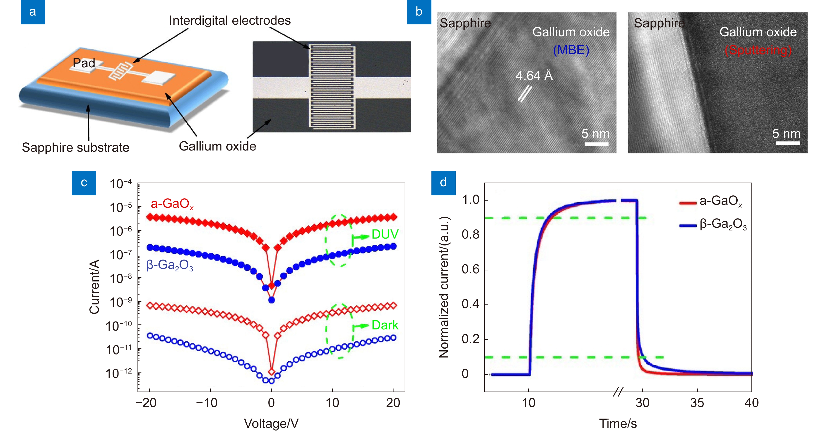
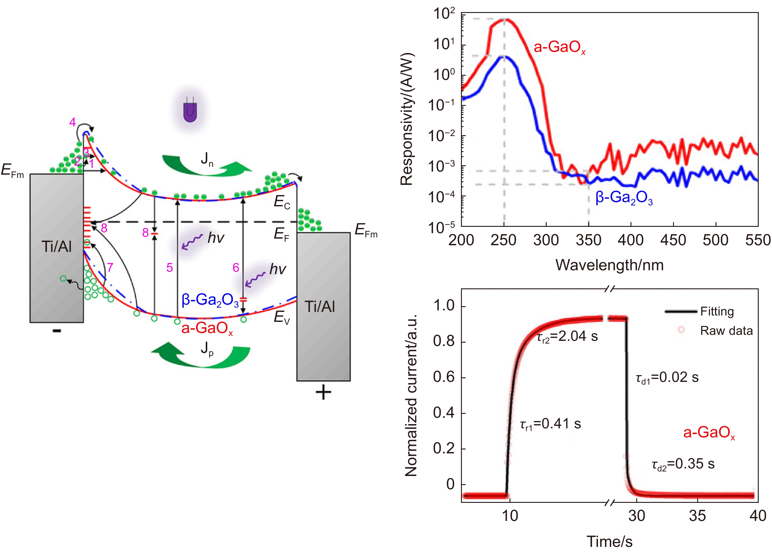
图 2 (a) 氧化镓MSM型日盲紫外探测器的结构示意图和实物照片;(b) 借助MBE和RFMS沉积的氧化镓薄膜的TEM图像;(c) 基于a-Ga2O3和β-Ga2O3的MSM型日盲紫外探测器的I-V特性曲线和(d)瞬态响应特性曲线[30]
Figure 2. (a) Schematic diagram and photograph of the gallium-oxide MSM photodetectors; (b) TEM images of the gallium oxide films deposited by RFMS and MBE; (c) I-V characteristics and (d) transient response of the MSM photodetectors based on a-Ga2O3 and β-Ga2O3 thin films[30]
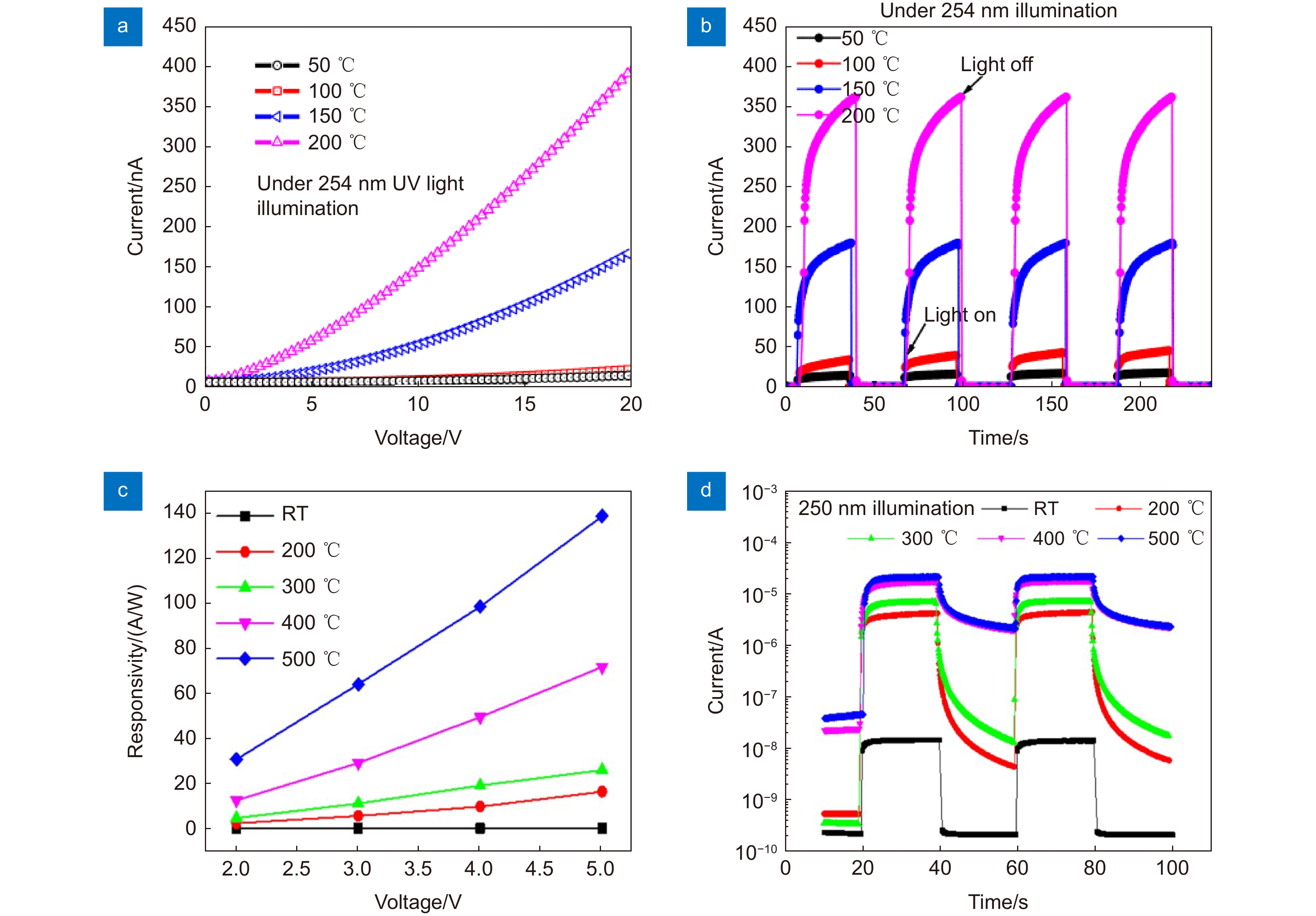
图 4 (a) 不同生长温度下制作的器件的I-V特性曲线与(b) I-T特性曲线[58];(c) 不同生长温度下制作的器件的响应度曲线与(d) I-T特性曲线[59]
Figure 4. (a) I−V characteristics and (b) I-T characteristics of the devices fabricated at various growth temperatures[58]; (c) Responsive characteristics and (d) I-T characteristics of the devices fabricated at various growth temperatures[59]
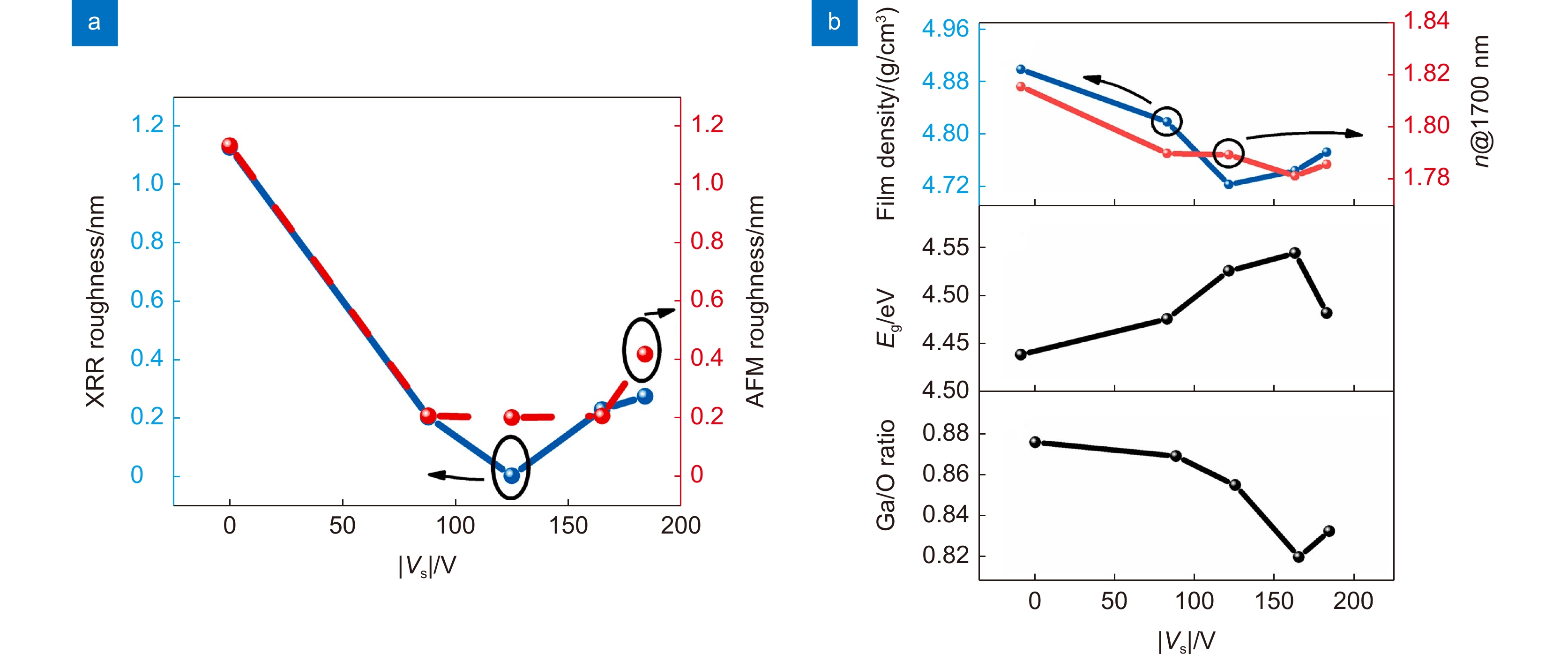
图 5 (a) XRR和AFM的薄膜粗糙度拟合结果;(b) 顶部:SE和XRR关于薄膜密度的拟合曲线。中间:a-GaOx带隙的变化趋势。底部:基于XPS分析的Ga/O比变化趋势[60]
Figure 5. (a) Film roughness fitting results from XRR and AFM; (b) Top: fitting curve of film density from SE and XRR. Medium: the variation trend of the a-GaOx bandgap. Bottom: Variation trend of Ga/O ratio based on XPS analysis[60]
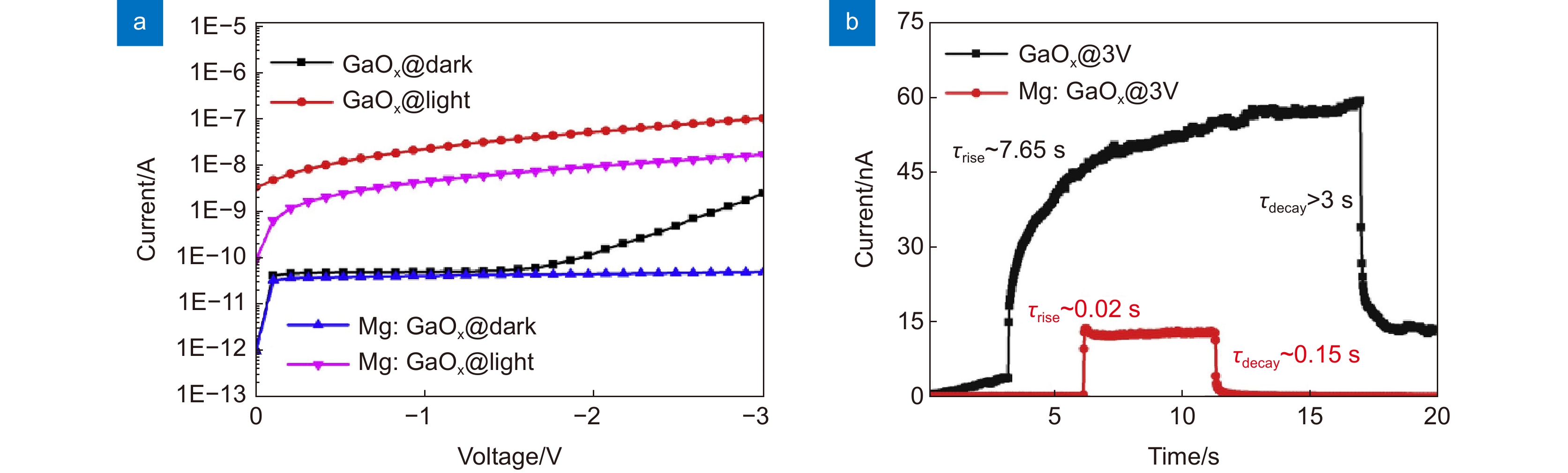
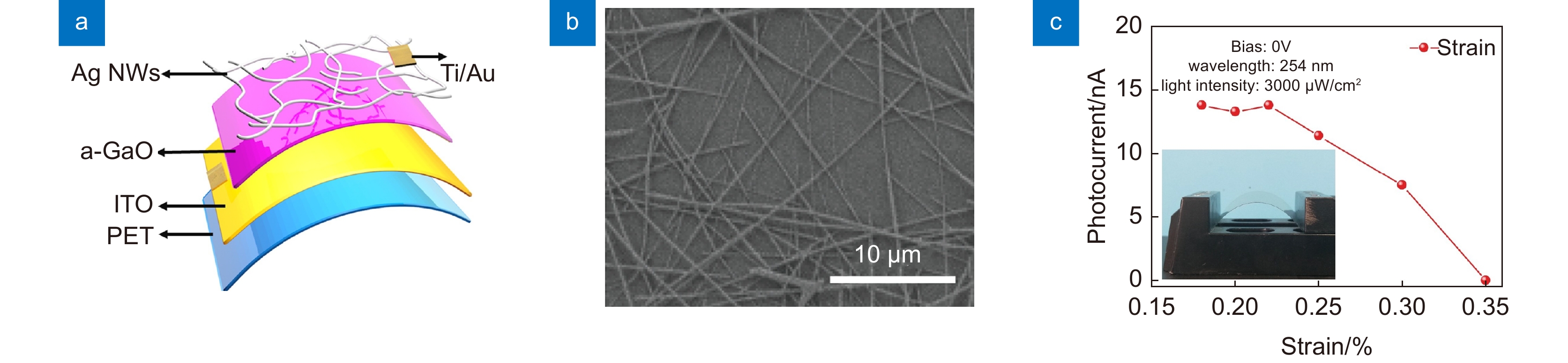
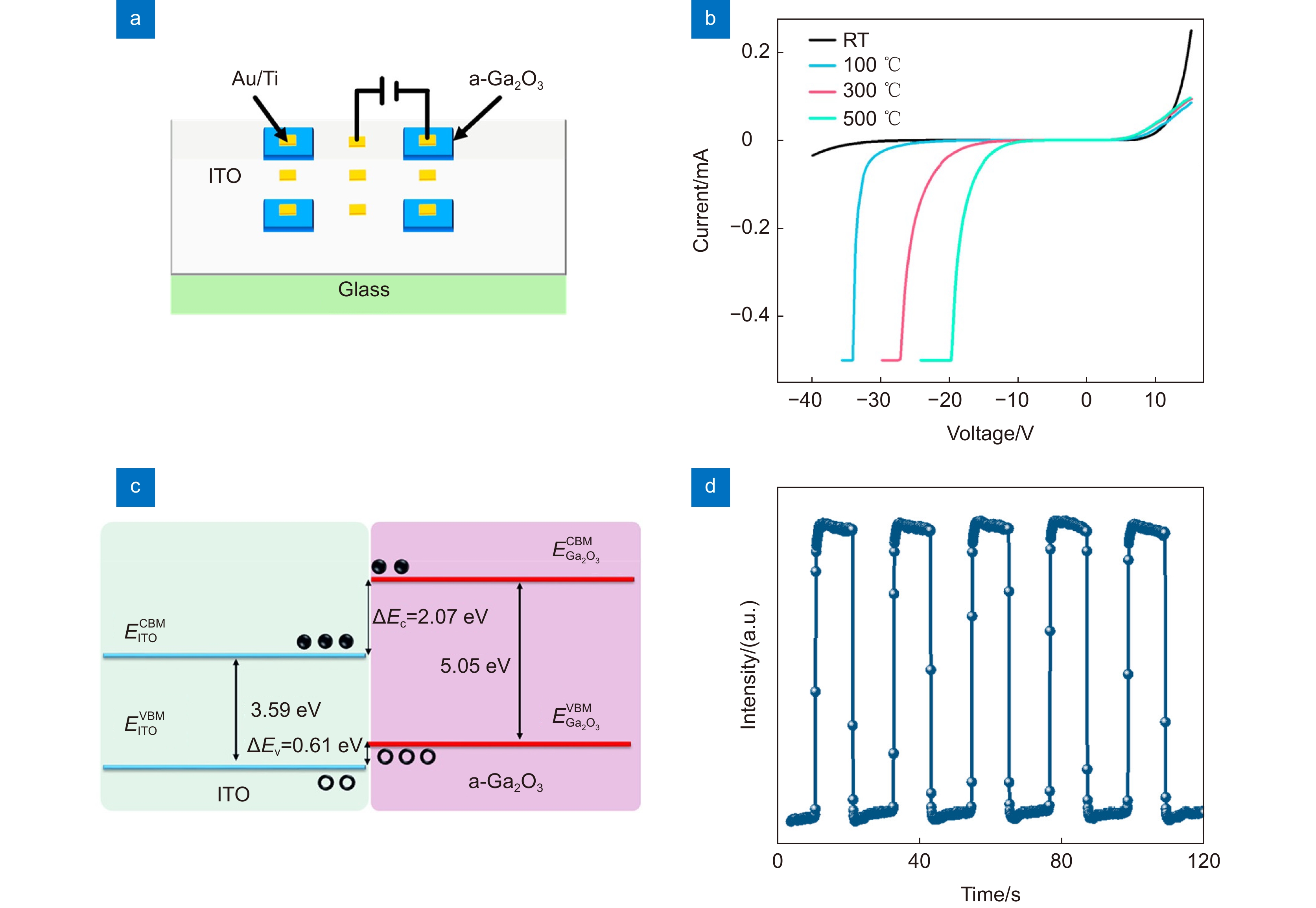
图 8 (a) a-Ga2O3/ITO器件示意图;(b) 不同生长温度下制作的器件的I-V特性曲线;(c) Ga2O3/ITO异质结的能带排列示意图;(d) 探测器的I-T特性曲线[70]
Figure 8. (a) Schematic of the a-Ga2O3/ITO prototype device; (b) I−V characteristics of the devices fabricated at various growth temperatures in dark; (c) Schematic of band alignment of the Ga2O3/ITO heterojunction; (d) The I–T characteristic of the detector[70]
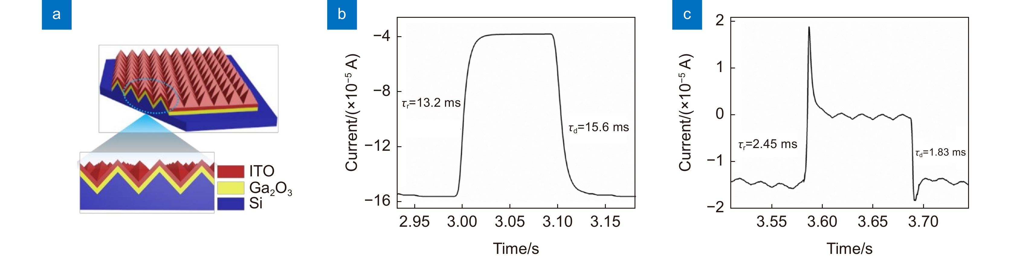
图 9 (a) a-Ga2O3/p-Si异质结光电探测器的示意图,放大图显示了该器件的横截面图;(b) 未经氧等离子体处理的器件的I-T特性曲线;(c) 经过氧等离子体处理的器件的I-T特性曲线[71]
Figure 9. (a) Schematic diagram of the a-Ga2O3/p-Si heterojunctions photodetector, the enlarged view shows a cross-sectional view of the device; (b) The I–T characteristic of the detector without oxygen plasma treatment; (c) The I–T characteristic of the detector with oxygen plasma treatment[71]
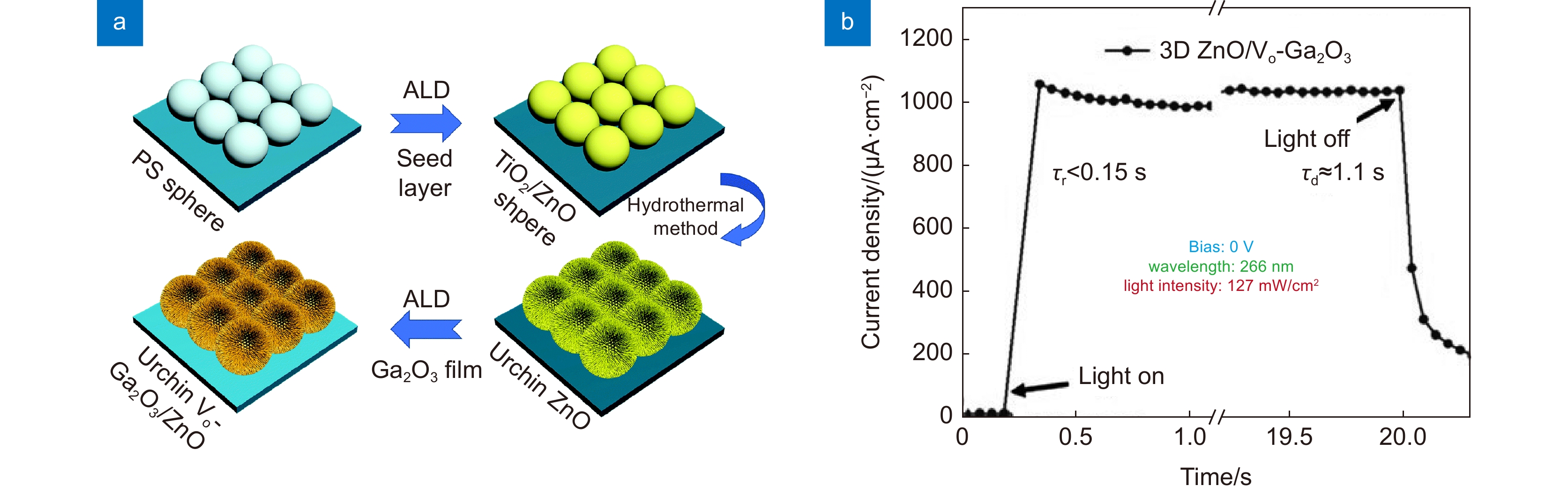
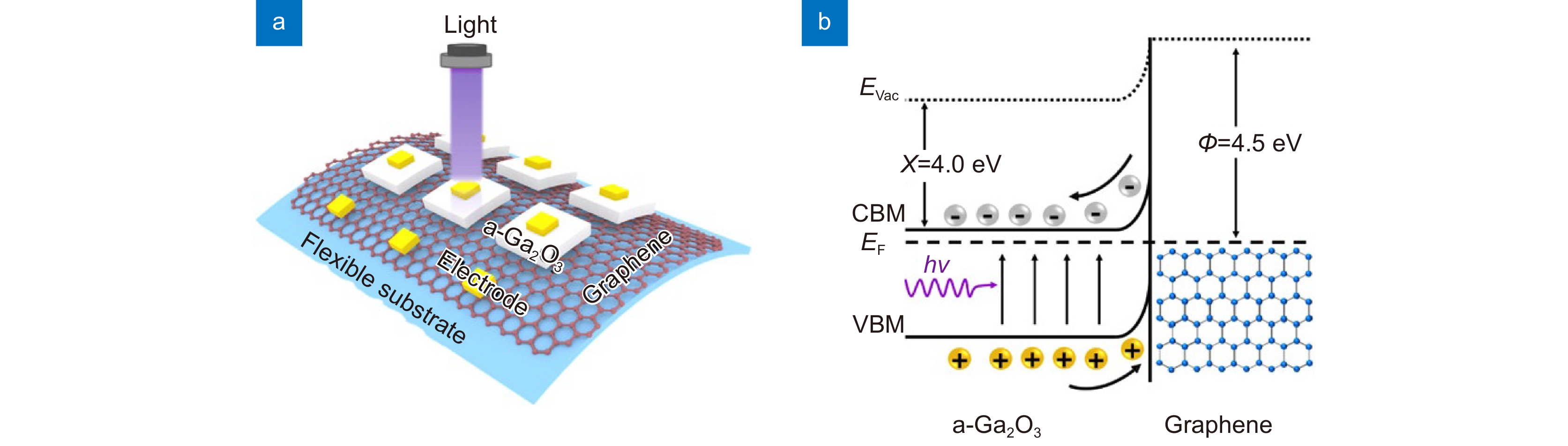
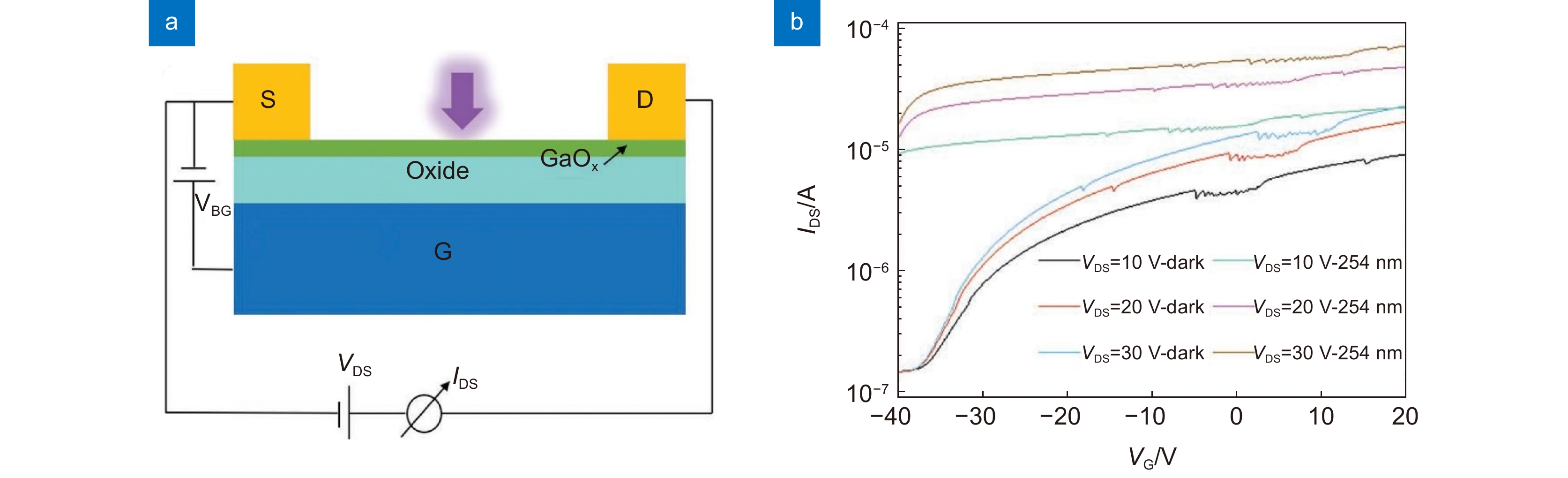
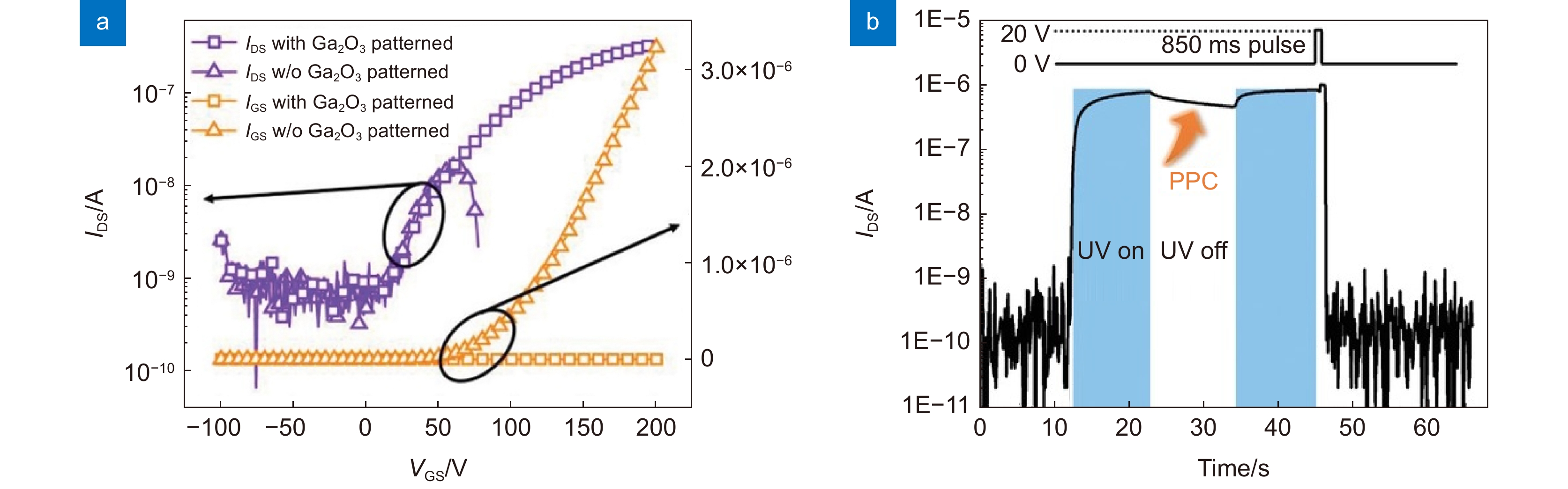
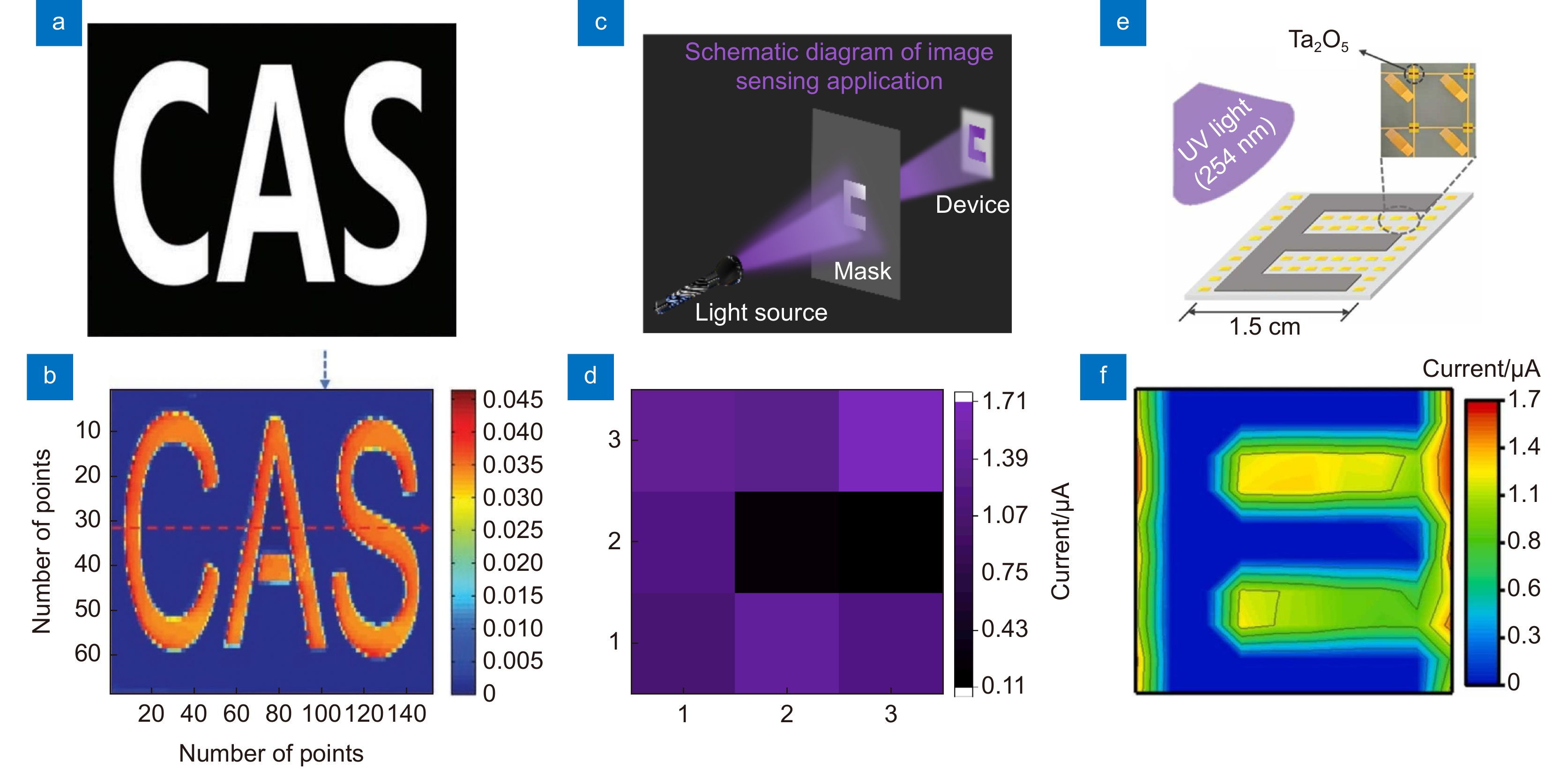
图 14 (a) 带有“CAS”字样的掩模版和(b)对应成像系统获得的图像[74];(c) 光学成像系统示意图以及(d)获得的“C”字图样[82];(e) 探测器阵列示意图以及(f)获得的“E”字图样[83]
Figure 14. (a) The photomask with letters “CAS” and (b) the image obtained from the imaging system[74]; (c) Schematic diagram of the optical imaging system and (d) the obtained "C" pattern [82]; (e) Schematic diagram of the PDs array and (f) the obtained "E" pattern [83]
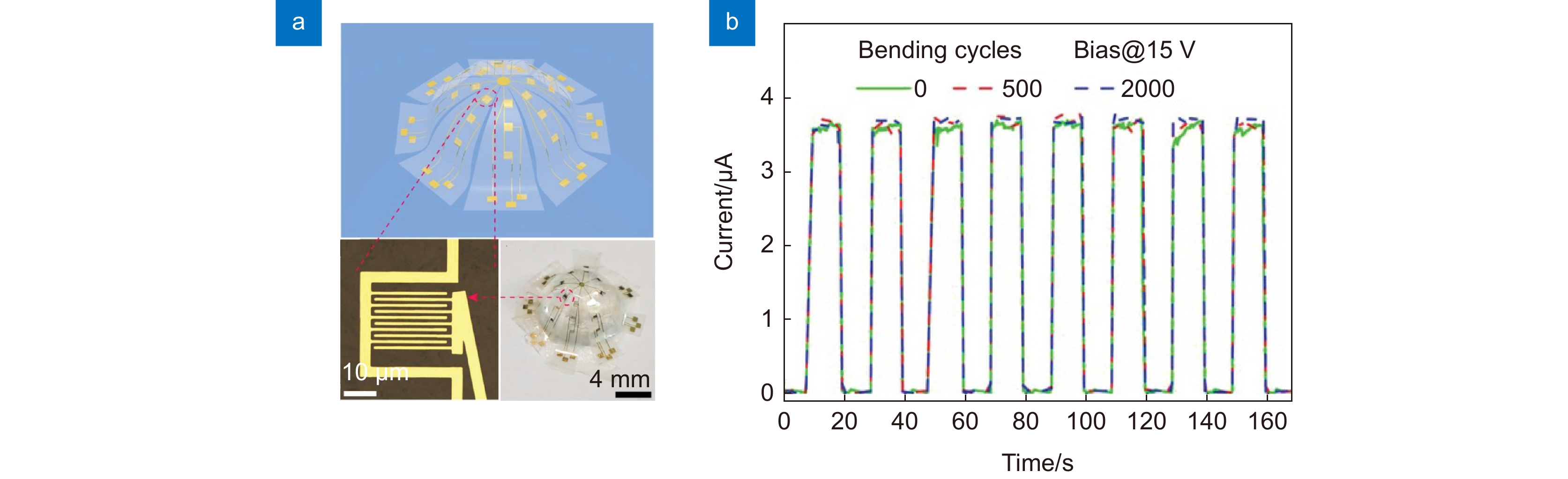
图 15 (a) 三维Ga2O3光电探测器阵列的示意图、实物照片以及单个光电探测器单元的显微镜图像;(b) 在不弯曲的情况下以及在500和2000次弯曲循环后,光电探测器在15 V偏压下的I-T曲线[80]
Figure 15. (a) Schematic of the 3D Ga2O3 photodetector array, photograph and microscope image of an individual photodetector cell; (b) I-T curves of the photodetector at 15 V without bending and after 500 and 2000 bending cycles[80]
表 1 a-Ga2O3日盲紫外探测器性能参数汇总
Table 1. Summary of parameters of recently reported a-Ga2O3 SBPDs
Structure Material Method Idark/nA R/(A/W) D*/(Jones) tr/s td/s Ref. MSM a-Ga2O3 RFMS 0.34 70.26 1.2×10¹⁴ 0.41/2.04 0.02/0.35 [30] a-Ga2O3 ALD 0.20 45.11 — 2.9×10⁻⁶ 1.48×10⁻⁴ [31] a-Ga2O3 RFMS ~10−3 0.19 — — 1.91/8.07×10−5 [32] a-Ga2O3 RFMS 4.9 436.3 — 8×10⁻⁸ 2.1×10⁻⁴ [57] a-Ga2O3 RFMS 49.4 138 — 0.52/3.88 0.32/4.00 [59] a-Ga2O3 ALD ~10−4 33.9 — 0.02/0.07 0.02/0.04 [61] a-Ga2O3 RFMS 1.27×10⁻³ 0.19 8.39×10¹³ 0.048/0.419 0.036 [62] In: a-Ga2O3 RFMS 0.029 0.26 — — 0.02/0.75 [33] In: a-Ga2O3 RFMS — 18.06 — 0.49/1.33×10−5 0.23/2.3×10−3 [63] Mg: a-Ga2O3 MOCVD 0.048 0.14 — ~0.02 ~0.15 [42] Tm: a-Ga2O3 PLD 0.036 0.447 2.26×10¹² 0.07 0.02 [64] a-Ga2O3 RFMS 0.11 43.99 — 6.14 2.32 [65] Junction a-Ga2O3/ITO RFMS ~1 5.9×10⁴ 1.8×10¹⁴ — — [70] a-Ga2O3/p-Si RFMS 1.04×10⁵ 9.97×10⁻³ — 2.45×10⁻³ 1.83×10⁻³ [71] a-Ga2O3/ZnO ALD — 7.97×10⁻³ 1.16×10¹¹ 0.15 1.1 [72] a-Ga2O3/GR RFMS ~10−3 22.75 8.2×10¹³ — — [73] TFT a-Ga2O3 RFMS 100 4.1×10³ 2.5×10¹³ 50 400 [74] a-Ga2O3 RFMS ~10−3 5.67×10³ 1.87×10¹⁵ — 5×10⁻³ [75] CdO: a-Ga2O3 SPD 1.61×10⁻³ 2.17 1.71×10¹² — — [76] a-Ga2O3 mist-CVD — 2.3×10³ 1.87×10¹⁴ 10 6 [77] a-Ga2O3 RFMS — 104 1×10¹⁵ — — [78] a-Ga2O3/IGZO RFMS ~10−4 4.8×10³ 8×10¹⁵ — 0.096 [79] Array a-Ga2O3 RFMS 0.17 8.9 — <1.5×10⁻⁵ 0.3/1.7×10−3 [80] a-Ga2O3 RFMS 3×10⁻⁴ 733 3.9×10¹⁶ <1×10⁻³ 0.018/0.091 [81] a-Ga2O3 RFMS 16.4 16.34 1.19×10¹³ 0.10/1.73 0.20/3.40 [82] a-Ga2O3 RFMS 6.6×10⁻³ 1021.8 1.66×10¹⁶ 0.144 0.208 [83]  下载: 导出CSV
-
[1] Xu J J, Zheng W, Huang F. Gallium oxide solar-blind ultraviolet photodetectors: a review[J]. J Mater Chem C, 2019, 7(29): 8753−8770. doi: 10.1039/C9TC02055A
[2] 徐国钧, 苏绍基. 紫外光电探测器的原理及其广泛应用[J]. 云南大学学报(自然科学版), 2001, 23(4): 275−278,282. doi: 10.3321/j.issn:0258-7971.2001.04.008
Xu G J, Su S J. The theory of ultravidet photodetector and extensive application[J]. J Yunnan Univ (Nat Sci Ed), 2001, 23(4): 275−278,282. doi: 10.3321/j.issn:0258-7971.2001.04.008
[3] Razeghi M, Rogalski A. Semiconductor ultraviolet detectors[J]. J Appl Phys, 1996, 79(10): 7433−7473. doi: 10.1063/1.362677
[4] Qin Y, Long S B, Dong H, et al. Review of deep ultraviolet photodetector based on gallium oxide[J]. Chin Phys B, 2019, 28(1): 018501. doi: 10.1088/1674-1056/28/1/018501
[5] Guo D Y, Su Y L, Shi H Z, et al. Self-powered ultraviolet photodetector with superhigh photoresponsivity (3.05 A/W) based on the GaN/Sn: Ga2O3 pn junction[J]. ACS Nano, 2018, 12(12): 12827−12835. doi: 10.1021/acsnano.8b07997
[6] Li Y B, Tokizono T, Liao M Y, et al. Efficient assembly of bridged β-Ga2O3 nanowires for solar-blind photodetection[J]. Adv Funct Mater, 2010, 20(22): 3972−3978. doi: 10.1002/adfm.201001140
[7] Pratiyush A S, Krishnamoorthy S, Solanke S V, et al. High responsivity in molecular beam epitaxy grown β-Ga2O3 metal semiconductor metal solar blind deep-UV photodetector[J]. Appl Phys Lett, 2017, 110(22): 221107. doi: 10.1063/1.4984904
[8] Chen M X, Zhao B, Hu G F, et al. Piezo-phototronic effect modulated deep UV photodetector based on ZnO-Ga2O3 heterojuction microwire[J]. Adv Funct Mater, 2018, 28(14): 1706379. doi: 10.1002/adfm.201706379
[9] Zhang W L, Çakıroğlu O, Al-Enizi A, et al. Solvent-free fabrication of broadband WS2 photodetectors on paper[J]. Opto-Electron Adv, 2023, 6: 220101. doi: 10.29026/oea.2023.220101
[10] Ohtsu M. History, current developments, and future directions of near-field optical science[J]. Opto-Electron Adv, 2020, 3(3): 190046. doi: 10.29026/oea.2020.190046
[11] Qian Y Z, Yang Z Y, Huang Y H, et al. Directional high-efficiency nanowire LEDs with reduced angular color shift for AR and VR displays[J]. Opto-Electron Sci, 2022, 1(12): 220021. doi: 10.29026/oes.2022.220021
[12] Min J H, Lee K, Chung T H, et al. Large-scale and high-quality III-nitride membranes through microcavity-assisted crack propagation by engineering tensile-stressed Ni layers[J]. Opto-Electron Sci, 2022, 1(10): 220016. doi: 10.29026/oes.2022.220016
[13] Yalagala B P, Dahiya A S, Dahiya R. ZnO nanowires based degradable high-performance photodetectors for eco-friendly green electronics[J]. Opto-Electron Adv, 2023, 6(2): 220020. doi: 10.29026/oea.2023.220020
[14] Chen Y R, Zhang Z W, Jiang H, et al. The optimized growth of AlN templates for back-illuminated AlGaN-based solar-blind ultraviolet photodetectors by MOCVD[J]. J Mater Chem C, 2018, 6(18): 4936−4942. doi: 10.1039/C8TC00755A
[15] Lu Y J, Lin C N, Shan C X. Optoelectronic diamond: growth, properties, and photodetection applications[J]. Adv Opt Mater, 2018, 6(20): 1800359. doi: 10.1002/adom.201800359
[16] Chen X, Liu K W, Wang X, et al. Performance enhancement of a ZnMgO film UV photodetector by HF solution treatment[J]. J Mater Chem C, 2017, 5(40): 10645−10651. doi: 10.1039/C7TC03352D
[17] Guo D Y, Wu Z P, Li P G, et al. Fabrication of β-Ga2O3 thin films and solar-blind photodetectors by laser MBE technology[J]. Opt Mater Express, 2014, 4(5): 1067−1076. doi: 10.1364/OME.4.001067
[18] Kong W Y, Wu G A, Wang K Y, et al. Graphene-β-Ga2O3 heterojunction for highly sensitive deep UV photodetector application[J]. Adv Mater, 2016, 28(48): 10725−10731. doi: 10.1002/adma.201604049
[19] Luan S Z, Dong L P, Jia R X. Analysis of the structural, anisotropic elastic and electronic properties of β-Ga2O3 with various pressures[J]. J Cryst Growth, 2019, 505: 74−81. doi: 10.1016/j.jcrysgro.2018.09.031
[20] Feng P, Zhang J Y, Li Q H, et al. Individual β-Ga2O3 nanowires as solar-blind photodetectors[J]. Appl Phys Lett, 2006, 88(15): 153107. doi: 10.1063/1.2193463
[21] Zou R J, Zhang Z Y, Liu Q, et al. High detectivity solar-blind high-temperature deep-ultraviolet photodetector based on multi-layered (l00) facet-oriented β-Ga2O3 nanobelts[J]. Small, 2014, 10(9): 1848−1856. doi: 10.1002/smll.201302705
[22] Oshima T, Okuno T, Arai N, et al. Vertical solar-blind deep-ultraviolet Schottky photodetectors based on β-Ga2O3 substrates[J]. Appl Phys Express, 2008, 1(1): 011202. doi: 10.1143/APEX.1.011202
[23] 侯爽, 刘庆, 邢志阳, 等. Sn掺杂对Ga2O3基日盲紫外探测器性能的影响研究[J]. 光电工程, 2019, 46(10): 190011. doi: 10.12086/oee.2019.190011
Hou S, Liu Q, Xing Z Y, et al. Effects of Sn doping on Ga2O3-based solar blind photodetectors[J]. Opto-Electron Eng, 2019, 46(10): 190011. doi: 10.12086/oee.2019.190011
[24] Suzuki R, Nakagomi S, Kokubun Y, et al. Enhancement of responsivity in solar-blind β-Ga2O3 photodiodes with a Au Schottky contact fabricated on single crystal substrates by annealing[J]. Appl Phys Lett, 2009, 94(22): 222102. doi: 10.1063/1.3147197
[25] Liu Z, Wang X, Liu Y Y, et al. A high-performance ultraviolet solar-blind photodetector based on a β-Ga2O3 Schottky photodiode[J]. J Mater Chem C, 2019, 7(44): 13920−13929. doi: 10.1039/C9TC04912F
[26] Liu Z, Li S, Yan Z Y, et al. Construction of a β-Ga2O3-based metal-oxide-semiconductor-structured photodiode for high-performance dual-mode solar-blind detector applications[J]. J Mater Chem C, 2020, 8(15): 5071−5081. doi: 10.1039/D0TC00100G
[27] Guo D Y, Zhao X L, Zhi Y S, et al. Epitaxial growth and solar-blind photoelectric properties of corundum-structured α-Ga2O3 thin films[J]. Mater Lett, 2016, 164: 364−367. doi: 10.1016/j.matlet.2015.11.001
[28] Pavesi M, Fabbri F, Boschi F, et al. ε-Ga2O3 epilayers as a material for solar-blind UV photodetectors[J]. Mater Chem Phys, 2018, 205: 502−507. doi: 10.1016/j.matchemphys.2017.11.023
[29] Teng Y, Song L X, Ponchel A, et al. Self-assembled metastable γ-Ga2O3 nanoflowers with hexagonal nanopetals for solar-blind photodetection[J]. Adv Mater, 2014, 26(36): 6238−6243. doi: 10.1002/adma.201402047
[30] Qian L X, Wu Z H, Zhang Y Y, et al. Ultrahigh-responsivity, rapid-recovery, solar-blind photodetector based on highly nonstoichiometric amorphous gallium oxide[J]. ACS Photonics, 2017, 4(9): 2203−2211. doi: 10.1021/acsphotonics.7b00359
[31] Lee S H, Kim S B, Moon Y J, et al. High-responsivity deep-ultraviolet-selective photodetectors using ultrathin gallium oxide films[J]. ACS Photonics, 2017, 4(11): 2937−2943. doi: 10.1021/acsphotonics.7b01054
[32] Cui S J, Mei Z X, Zhang Y H, et al. Room-temperature fabricated amorphous Ga2O3 high-response-speed solar-blind photodetector on rigid and flexible substrates[J]. Adv Opt Mater, 2017, 5(19): 1700454. doi: 10.1002/adom.201700454
[33] Chen K Y, Hsu C C, Yu H C, et al. The effect of oxygen vacancy concentration on indium gallium oxide solar blind photodetector[J]. IEEE Trans Electron Devices, 2018, 65(5): 1817−1822. doi: 10.1109/TED.2018.2817637
[34] Stepanov S I, Nikolaev V I, Bougrov V E, et al. Gallium oxide: properties and applications-a review[J]. Rev Adv Mater Sci, 2016, 44(1): 63−86.
[35] Yu F P, Ou S L, Wuu D S. Pulsed laser deposition of gallium oxide films for high performance solar-blind photodetectors[J]. Opt Mater Express, 2015, 5(5): 1240−1249. doi: 10.1364/OME.5.001240
[36] Wang Y H, Cui W J, Yu J, et al. One-step growth of amorphous/crystalline Ga2O3 phase junctions for high-performance solar-blind photodetection[J]. ACS Appl Mater Interfaces, 2019, 11(49): 45922−45929. doi: 10.1021/acsami.9b17409
[37] Nieminen M, Niinistö L, Rauhala E. Growth of gallium oxide thin films from gallium acetylacetonate by atomic layer epitaxy[J]. J Mater Chem, 1996, 6(1): 27−31. doi: 10.1039/JM9960600027
[38] Kim N H, Kim H W, Chang S, et al. Amorphous gallium oxide nanowires synthesized by metalorganic chemical vapor deposition[J]. Mater Sci Eng B, 2004, 111(2–3): 131−134. doi: 10.1016/j.mseb.2004.04.002
[39] Zhao J L, Sun X W, Ryu H, et al. UV and visible electroluminescence from a Sn: Ga2O3/n+-Si heterojunction by metal–organic chemical vapor deposition[J]. IEEE Trans Electron Devices, 2011, 58(5): 1447−1451. doi: 10.1109/TED.2011.2112364
[40] Takiguchi Y, Miyajima S. Effect of post-deposition annealing on low temperature metalorganic chemical vapor deposited gallium oxide related materials[J]. J Cryst Growth, 2017, 468: 129−134. doi: 10.1016/j.jcrysgro.2016.11.005
[41] Kobayashi E, Boccard M, Jeangros N, et al. Amorphous gallium oxide grown by low-temperature PECVD[J]. J Vac Sci Technol A, 2018, 36(2): 021518. doi: 10.1116/1.5018800
[42] Zhang D, Du Z, Ma M H, et al. Enhanced performance of solar-blind ultraviolet photodetector based on Mg-doped amorphous gallium oxide film[J]. Vacuum, 2019, 159: 204−208. doi: 10.1016/j.vacuum.2018.10.025
[43] Guo D Y, Wu Z P, An Y H, et al. Unipolar resistive switching behavior of amorphous gallium oxide thin films for nonvolatile memory applications[J]. Appl Phys Lett, 2015, 106(4): 042105. doi: 10.1063/1.4907174
[44] Shi Q, Wang Q R, Zhang D, et al. Structural, optical and photoluminescence properties of Ga2O3 thin films deposited by vacuum thermal evaporation[J]. J Lumin, 2018, 206: 53−58. doi: 10.1016/j.jlumin.2018.10.005
[45] Kalygina V M, Vishnikina V V, Zarubin A N, et al. Effect of annealing in argon on the properties of thermally deposited gallium-oxide films[J]. Semiconductors, 2013, 47(8): 1130−1136. doi: 10.1134/S1063782613080071
[46] Rao P, Kumar S. Influence of post-deposition annealing in air and vacuum on the properties of thermally evaporated gallium oxide films[J]. Superlattices Microstruct, 2014, 70: 117−130. doi: 10.1016/j.spmi.2014.03.009
[47] Yi C, Liang H W, Yang L, et al. Influence of N2 and O2 annealing treatment on the optical bandgap of polycrystalline Ga2O3: Cu films[J]. Mater Sci Semicond Process, 2013, 16(5): 1303−1307. doi: 10.1016/j.mssp.2013.03.003
[48] Cabello G, Lillo L, Caro C, et al. Evaluation on the optical properties of Ga2O3-x thin films co-doped with Tb3+ and transition metals (Mn2+, Cr3+) prepared by a photochemical route[J]. Ceram Int, 2013, 39(3): 2443−2450. doi: 10.1016/j.ceramint.2012.08.096
[49] Cabello G, Araneda A, Lillo L, et al. Application of photochemical method in the synthesis of Ga2O3-X thin films co-doped with terbium and europium[J]. Solid State Sciences, 2014, 27: 24−29. doi: 10.1016/j.solidstatesciences.2013.11.002
[50] Petitmangin A, Hébert C, Perrière J, et al. Metallic clusters in nonstoichiometric gallium oxide films[J]. J Appl Phys, 2011, 109(1): 013711. doi: 10.1063/1.3531536
[51] Hebert C, Petitmangin A, Perrière J, et al. Phase separation in oxygen deficient gallium oxide films grown by pulsed-laser deposition[J]. Mater Chem Phys, 2012, 133(1): 135−139. doi: 10.1016/j.matchemphys.2011.12.078
[52] Kumar S S, Rubio E J, Noor-A-Alam M, et al. Structure, morphology, and optical properties of amorphous and nanocrystalline gallium oxide thin films[J]. J Phys Chem C, 2013, 117(8): 4194−4200. doi: 10.1021/jp311300e
[53] Ramana C V, Rubio E J, Barraza C D, et al. Chemical bonding, optical constants, and electrical resistivity of sputter-deposited gallium oxide thin films[J]. J Appl Phys, 2014, 115(4): 043508. doi: 10.1063/1.4862186
[54] Li X, Lu H L, Ma H P, et al. Chemical, optical, and electrical characterization of Ga2O3 thin films grown by plasma-enhanced atomic layer deposition[J]. Curr Appl Phys, 2019, 19(2): 72−81. doi: 10.1016/j.cap.2018.11.013
[55] 韩祖银. 非晶氧化镓基光电晶体管和成像系统研究[D]. 北京: 中国科学院大学 (中国科学院物理研究所), 2021. https://doi.org/10.27604/d.cnki.gwlys.2021.000061.
Han Z Y. Research on amorphous gallium oxide based phototransistor and imaging system[D]. Beijing: Institute of Physics, Chinese Academy of Sciences, 2021. https://doi.org/10.27604/d.cnki.gwlys.2021.000061.
[56] Zhang Y F, Chen X H, Xu Y, et al. Transition of photoconductive and photovoltaic operation modes in amorphous Ga2O3-based solar-blind detectors tuned by oxygen vacancies[J]. Chin Phys B, 2019, 28(2): 028501. doi: 10.1088/1674-1056/28/2/028501
[57] Han S, Huang X L, Fang M Z, et al. High-performance UV detectors based on room-temperature deposited amorphous Ga2O3 thin films by RF magnetron sputtering[J]. J Mater Chem C, 2019, 7(38): 11834−11844. doi: 10.1039/C9TC03613J
[58] Li Z, Xu Y, Zhang J Q, et al. Flexible solar-blind Ga2O3 ultraviolet photodetectors with high responsivity and photo-to-dark current ratio[J]. IEEE Photonics J, 2019, 11(6): 1−9. doi: 10.1109/jphot.2019.2946731
[59] Zhu W H, Xiong L X, Si J W, et al. Influence of deposition temperature on amorphous Ga2O3 solar-blind ultraviolet photodetector[J]. Semicond Sci Technol, 2020, 35(5): 055037. doi: 10.1088/1361-6641/ab6ac1
[60] Pei Y, Liang L Y, Wang X L, et al. Substrate-bias-aided preparation and properties of amorphous gallium oxide films and their deep-ultraviolet photodetectors[J]. Ceram Int, 2021, 47(22): 32138−32143. doi: 10.1016/j.ceramint.2021.08.105
[61] Yang Y, Liu W M, Huang T T, et al. Low Deposition temperature amorphous ALD-Ga2O3 thin films and decoration with mos2 multilayers toward flexible solar-blind photodetectors[J]. ACS Appl Mater Interfaces, 2021, 13(35): 41802−41809. doi: 10.1021/acsami.1c11692
[62] Zhang T, Guan D G, Liu N T, et al. Room temperature fabrication and post-annealing treatment of amorphous Ga2O3 photodetectors for deep-ultraviolet light detection[J]. Appl Phys Express, 2022, 15(2): 022007. doi: 10.35848/1882-0786/ac48d9
[63] Fang M Z, Zhao W G, Li F F, et al. Fast response solar-blind photodetector with a quasi-Zener tunneling effect based on amorphous in-doped Ga2O3 thin films[J]. Sensors, 2019, 20(1): 129. doi: 10.3390/s20010129
[64] Qu Q L, Liu Q, Chen L F, et al. Flexible fast responding solar-blind photodetectors based on (TmGa)2O3 films grown on mica[J]. Appl Phys Lett, 2022, 120(12): 122108. doi: 10.1063/5.0088714
[65] Kumar N, Arora K, Kumar M. High performance, flexible and room temperature grown amorphous Ga2O3 solar-blind photodetector with amorphous indium-zinc-oxide transparent conducting electrodes[J]. J Phys D Appl Phys, 2019, 52(33): 335103. doi: 10.1088/1361-6463/ab236f
[66] 玄鑫淼, 王加恒, 毛彦琦, 等. 基于云母衬底生长的非晶Ga2O3柔性透明日盲紫外光探测器研究[J]. 物理学报, 2021, 70(23): 238502. doi: 10.7498/aps.70.20211039
Xuan X M, Wang J H, Mao Y Q, et al. Flexible transparent solar blind ultraviolet photodetector based on amorphous Ga2O3 grown on mica substrate[J]. Acta Phys Sin, 2021, 70(23): 238502. doi: 10.7498/aps.70.20211039
[67] Xiao S Y, Deng Y, Chen Z Y, et al. Flexible and highly stable solar-blind photodetector based on room-temperature synthesis of amorphous Ga2O3 film[J]. J Phys D Appl Phys, 2020, 53(48): 484004. doi: 10.1088/1361-6463/abad64
[68] Wang S L, Wu C, Wu F M, et al. Flexible, transparent and self-powered deep ultraviolet photodetector based on Ag NWs/amorphous gallium oxide Schottky junction for wearable devices[J]. Sens Actuators A Phys, 2021, 330: 112870. doi: 10.1016/j.sna.2021.112870
[69] Xiong L X, Zhang L, Lv Q P, et al. Amorphous gallium oxide (a-Ga2O3)-based high-temperature bendable solar-blind ultraviolet photodetector[J]. Semicond Sci Technol, 2021, 36(4): 045010. doi: 10.1088/1361-6641/abe42c
[70] Wang Y H, Li H R, Cao J, et al. Ultrahigh gain solar blind avalanche photodetector using an amorphous Ga2O3-based heterojunction[J]. ACS Nano, 2021, 15(10): 16654−16663. doi: 10.1021/acsnano.1c06567
[71] Cao J, Chen L, Chen X, et al. Performance improvement of amorphous Ga2O3/P-Si deep ultraviolet photodetector by oxygen plasma treatment[J]. Crystals, 2021, 11(10): 1248. doi: 10.3390/cryst11101248
[72] Ni D W, Wang Y J, Li A S, et al. ALD oxygen vacancy-rich amorphous Ga2O3 on three-dimensional urchin-like ZnO arrays for high-performance self-powered solar-blind photodetectors[J]. Nanoscale, 2022, 14(8): 3159−3165. doi: 10.1039/D1NR08262K
[73] Wang Y H, Yang Z B, Li H R, et al. Ultrasensitive flexible solar-blind photodetectors based on graphene/amorphous Ga2O3 van der Waals heterojunctions[J]. ACS Appl Mater Interfaces, 2020, 12(42): 47714−47720. doi: 10.1021/acsami.0c10259
[74] Qin Y, Long S B, He Q M, et al. Amorphous gallium oxide-based gate-tunable high-performance thin film phototransistor for solar-blind imaging[J]. Adv Electron Mater, 2019, 5(7): 1900389. doi: 10.1002/aelm.201900389
[75] Han Z Y, Liang H L, Huo W X, et al. Boosted UV photodetection performance in chemically etched amorphous Ga2O3 thin-film transistors[J]. Adv Opt Mater, 2020, 8(8): 1901833. doi: 10.1002/adom.201901833
[76] Xiao X, Liang L Y, Pei Y, et al. Solution-processed amorphous Ga2O3: CdO TFT-type deep-UV photodetectors[J]. Appl Phys Lett, 2020, 116(19): 192102. doi: 10.1063/5.0007617
[77] Xu Y, Cheng Y L, Li Z, et al. High-performance gate tunable solar blind ultraviolet phototransistors based on amorphous Ga2O3 films grown by mist chemical vapor deposition[J]. Nano Select, 2021, 2(11): 2112−2120. doi: 10.1002/nano.202100029
[78] Pintor-Monroy M I, Reyes-Banda M G, Avila-Avendano C, et al. Tuning electrical properties of amorphous Ga2O3 thin films for deep UV phototransistors[J]. IEEE Sensors J, 2021, 21(13): 14807−14814. doi: 10.1109/JSEN.2021.3074623
[79] Han Z Y, Song S, Liang H L, et al. High-performance IGZO/Ga2O3 dual-active-layer thin film transistor for deep UV detection[J]. Appl Phys Lett, 2022, 120(26): 262102. doi: 10.1063/5.0089038
[80] Chen Y C, Lu Y J, Liao M Y, et al. 3D solar-blind Ga2O3 photodetector array realized via origami method[J]. Adv Funct Mater, 2019, 29(50): 1906040. doi: 10.1002/adfm.201906040
[81] Qin Y, Li L H, Yu Z A, et al. Ultra-high performance amorphous Ga2O3 photodetector arrays for solar-blind imaging[J]. Adv Sci, 2021, 8(20): 2101106. doi: 10.1002/advs.202101106
[82] Huang Z H, Zhou S R, Chen L R, et al. Fully transparent amorphous Ga2O3-based solar-blind ultraviolet photodetector with graphitic carbon electrodes[J]. Crystals, 2022, 12(10): 1427. doi: 10.3390/cryst12101427
[83] Ji X Q, Yin X M, Yuan Y Z, et al. Amorphous Ga2O3 Schottky photodiodes with high-responsivity and photo-to-dark current ratio[J]. J Alloys Comp, 2023, 933: 167735. doi: 10.1016/j.jallcom.2022.167735
-
 点击扫一扫
点击扫一扫
图(16)
表(1)
计量
- 文章访问数: 8429
- PDF下载数: 2596
- 施引文献: 0


