
 E-mail Alert
 RSS
RSS
Femtosecond laser two-photon polymerization three-dimensional micro-nanofabrication technology
-
摘要:
飞秒激光双光子聚合微纳加工技术作为重要的三维微纳结构制备手段,已成为国际前沿研究热点。该技术利用激光与物质相互作用的双光子非线性吸收效应和阈值效应,可以突破经典光学理论衍射极限,实现纳米尺度的激光加工分辨力,在三维功能性微纳器件制备领域正在发挥着十分重要的作用。本文在介绍飞秒激光双光子聚合三维微纳加工技术的光物理和光化学过程基本原理的基础上,重点回顾人们在改善加工线宽及分辨力、提高加工效率等方面的研究进展与发展概况。该技术所制备的各种微光学器件、集成光学器件、微机电系统以及生物医学器件,不仅充分展示了飞秒激光双光子聚合三维微纳加工技术的高空间分辨力和真三维加工特点,也为其在相关前沿领域的应用提供具有启发性的思路。最后,对该技术实现高精度、高效率、低成本、大面积、多功能的三维微纳结构加工所存在的挑战和未来发展方向,进行了讨论和展望。
Abstract:Femtosecond laser two-photon polymerization (TPP) micro-nano fabrication technology, as an important method for the preparation of three-dimensional (3D) micro-nanostructures, has become a hot spot of international frontier research. Using the two-photon absorption effect and the threshold effect of the interaction between laser and matter, this technology can break through the diffraction limit of classical optical theory and achieve nanoscale laser fabrication resolution. It is expected to play an important role in the field of 3D functional micro-nano device fabrication. In this paper, the basic principles of photophysical and photochemical processes in femtosecond pulsed laser TPP fabrication technology will be described, and the research progress and development of this technology in improving line width and fabrication resolution, and improving fabrication efficiency will be reviewed. Then, using the high spatial resolution and true 3D fabrication characteristics of femtosecond laser TPP micro-nano fabrication technology, the researchers prepared various micro-optical devices, integrated optical devices, micro-electromechanical systems, and biomedical devices, fully demonstrating the application prospect of this technology. Finally, how to achieve high-precision, high-efficiency, low-cost, large-area, multi-functional materials and microstructure fabrication, as well as existing challenges and future development directions are discussed and prospected.
-
Key words:
- femtosecond laser /
- two-photon polymerization /
- optical diffraction limit /
- resolution /
- efficiency
-
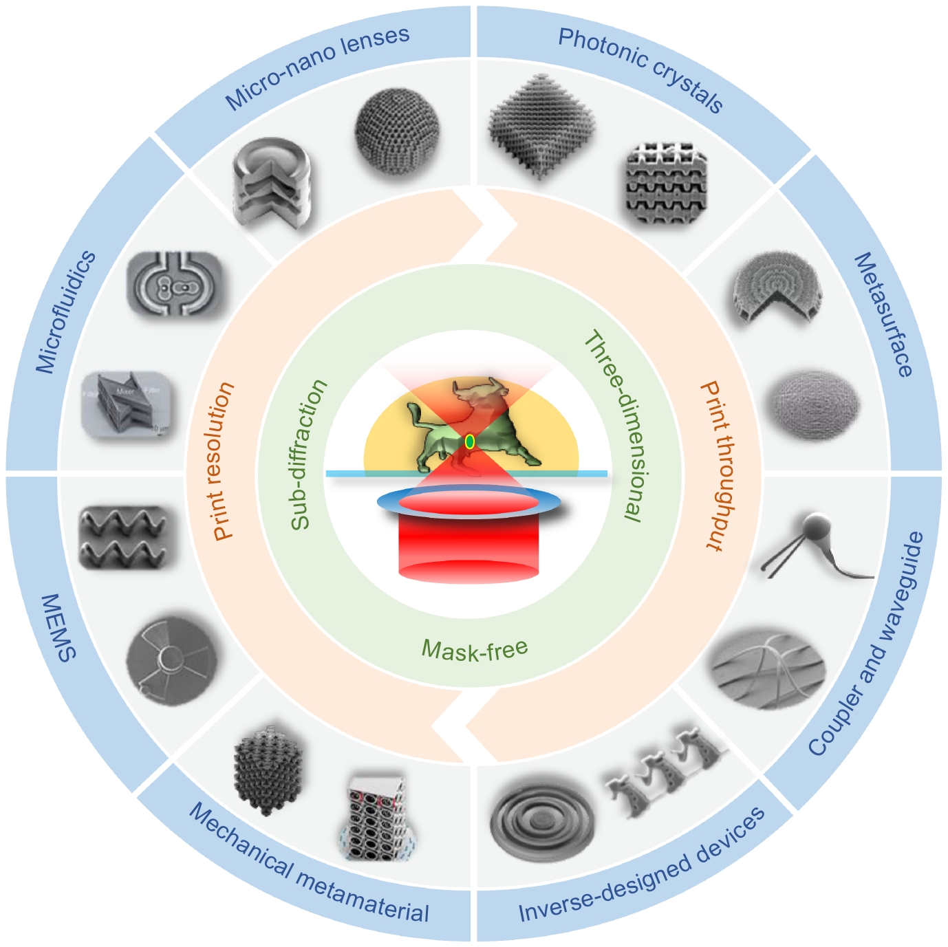
Overview: Femtosecond laser two-photon polymerization (TPP) micro-nanofabrication technology is a new type of three-dimensional lithography technology that integrates nonlinear optics, ultra-fast pulsed laser, microscopic imaging, ultra-high-precision positioning, three-dimensional (3D) graphics CAD modeling, and photochemical materials. It has the characteristics of simplicity, low cost, high resolution, true 3D, and so on. Different from the technical route of shortening the wavelength of the traditional lithography, this TPP technology breaks through the optical diffraction limit using the ultrafast laser in the near-infrared and the nonlinear optical effect of the interaction between the laser and the material. TPP can achieve true 3D fabrication of complex 3D structures. After the femtosecond pulse laser is tightly focused in space, photopolymerization is initiated by the two-photon absorption(TPA), which can limit the fabrication area in the center of the focus. The interaction time of the ultrashort pulse with the material is much lower than the thermal relaxation of the material, avoiding the photothermal effect. The lateral linewidth can be reduced to about 100 nm due to the strong threshold characteristics of the two-photon absorption process. Thus, TPP is an ideal fabrication method in the field of 3D micro-nanostructure. Since 2001, Kawata’s team has used a near-infrared femtosecond laser with a wavelength of 780 nm to fabricate a "nanobull" with the size of red blood cells. It fully demonstrated the advantages of TPP in the preparation of three-dimensional micro-nano structures. At the same time, a polymer nanodot with a size of 120 nm was fabricated, which was only 1/7 of the laser wavelength, breaking the optical diffraction limit in this study. Since then, scientists from various countries have improved the line width, resolution, and other parameters of 3D structure by continuously improving the materials, structure, processing technology and light field control, and other aspects. At the same time, with the continuous development and improvement of the 3D nanostructure fabrication technology, the advantages of TPP technology are also reflected in some application fields, such as micro-optical devices, integrated optical devices, micro-electromechanical systems, and biomedical devices. This paper will systematically introduce the femtosecond laser TPP micro-nanofabrication technology, including the fabricating principle, the development of fabricating methods, and its research overview in many application fields. Finally, its existing problems and future development and application prospects are discussed.
-

-
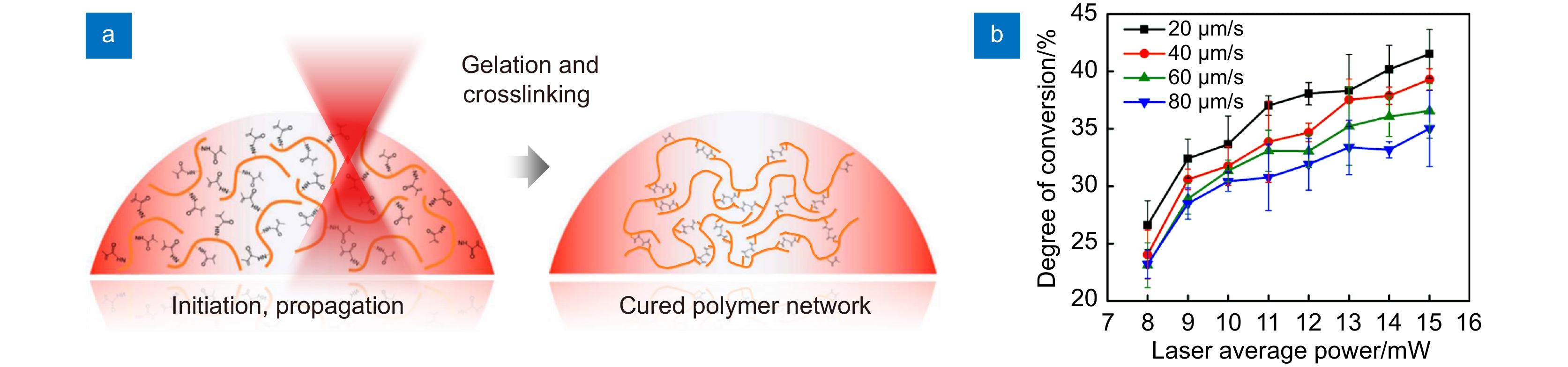
图 2 光聚合交联过程及单体转化度。(a) 光刻胶中单体分子聚合和交联过程示意图[64]; (b) 在商业(丙烯酸酯基)光刻胶 IP-L 780 中不同扫描速度下拉曼光谱计算的单体转化度[67]
Figure 2. Cross-linking process and degree of conversion. (a) Schematic diagram of the polymerization and cross-linking process of monomer molecules[64]; (b) Degree of conversion calculated from the Raman spectra for TPP with different scanning velocities in the commercial (acrylate-based) photoresist IP-L 780[67]
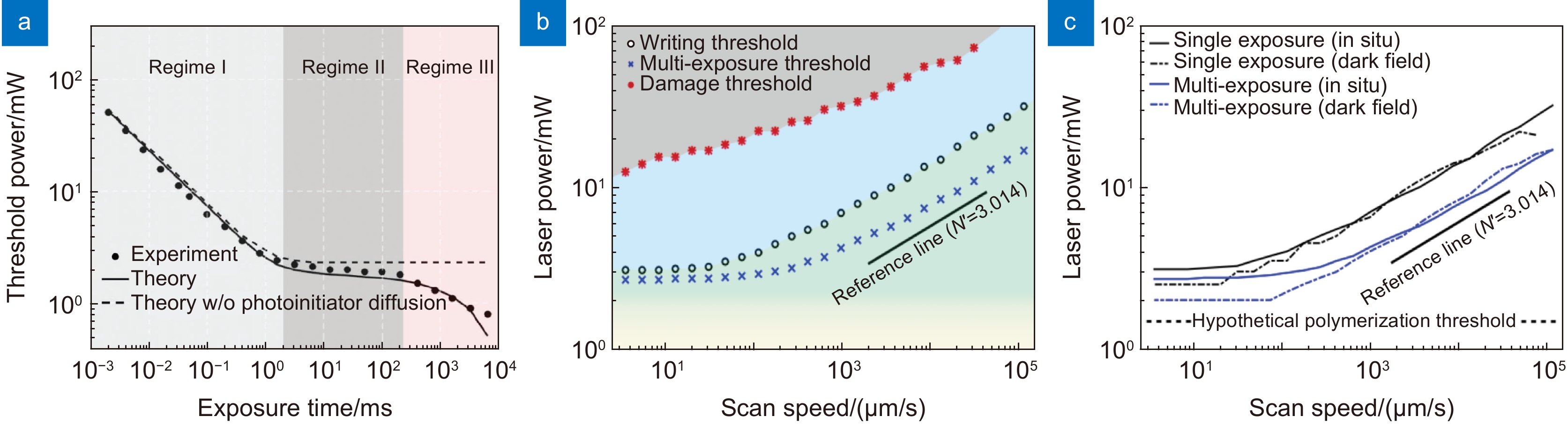
图 3 光聚合阈值和破坏阈值分布图。(a) 激光曝光阈值强度随着曝光时间变化关系[71];(b) 暗场显微镜测量的不同扫描速度下聚合阈值和破坏阈值激光强度[47];(c) 暗场和原位显微镜测量单次和多次曝光下阈值激光强度[47]
Figure 3. Distribution of the photopolymerization threshold and the damage threshold. (a) Laser exposure threshold intensity as a function of exposure time[71]; (b) Laser power threshold at different scan speeds measured by darkfield microscopy[47]; (c) Threshold laser intensities at single and multiple exposures measured by darkfield and in situ microscopy[47]
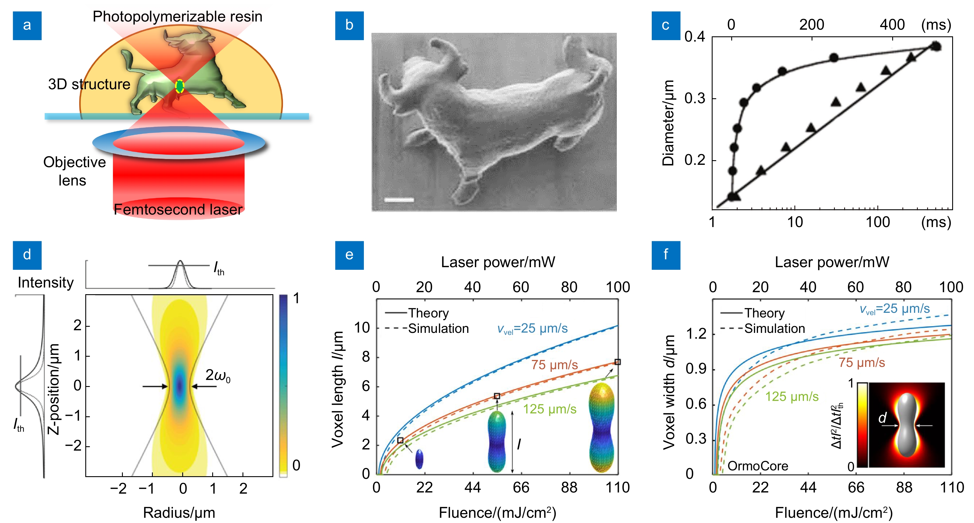
图 4 双光子聚合加工超衍射特征尺寸结构,以及加工聚合体元(Voxel)形貌模型。(a) 双光子聚合加工示意图[15];(b) 制备的“纳米牛”[19];(c) 线宽与曝光时间的非线性关系[19];(d) 双光子聚合加工焦点处光强度分布,其中虚线为光强度的平方[47];(e) 体元长度与曝光功率关系[78];(f) 体元线宽与曝光功率关系[78]
Figure 4. Sub-diffractive feature-scale structures by TPP and topography models of Voxel. (a) Schematic diagram of the TPP[15]; (b) The prepared "nano bull"[19]; (c) The nonlinear relationship between line width and exposure time[19]; (d) Light intensity distribution of the focus, where the dotted line is the square of light intensity[47]; (e) The relationship between voxel length and exposure power[78]; (f) The relationship between voxel linewidth and exposure power[78]
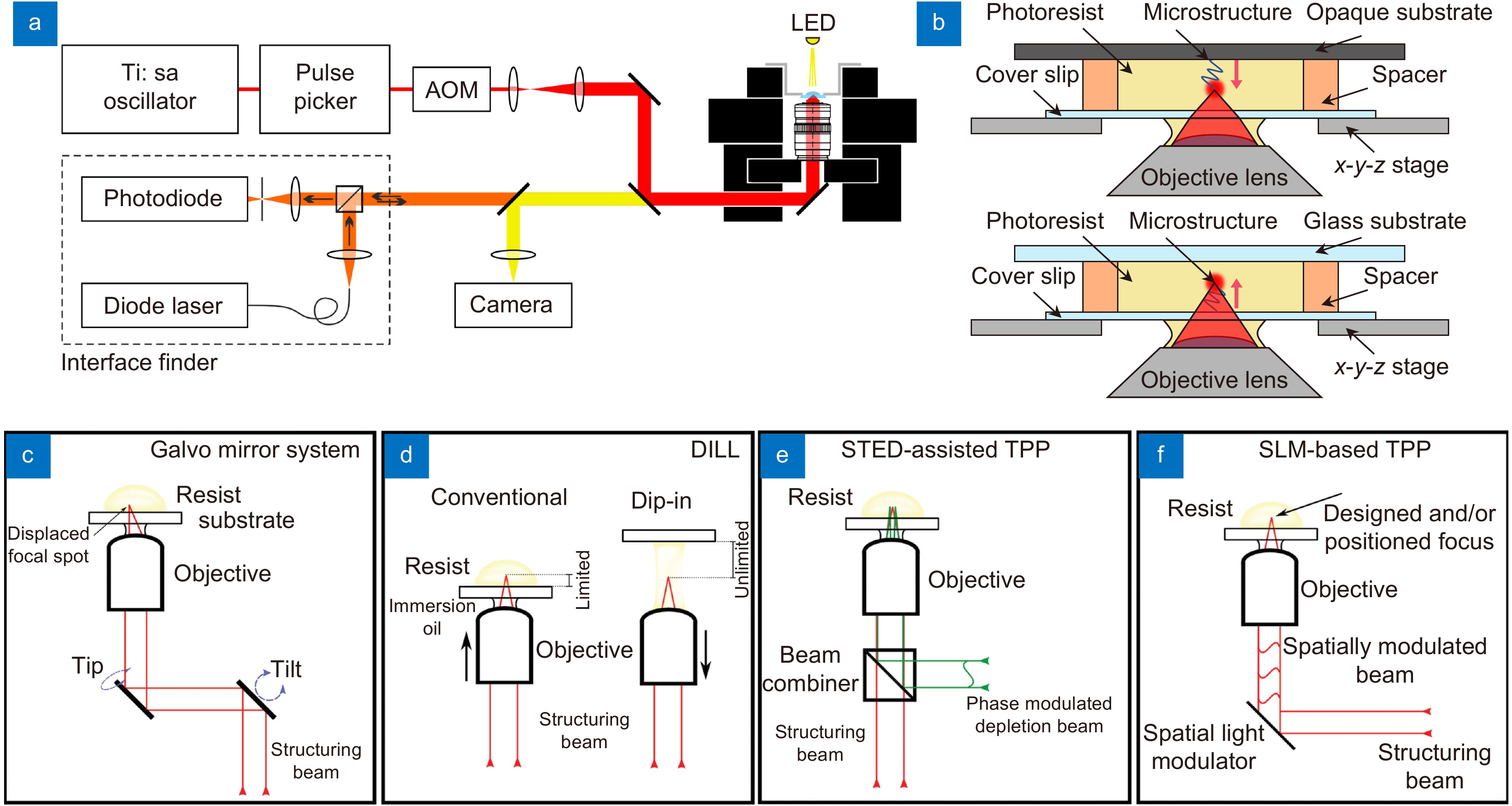
图 5 双光子聚合加工系统示意图。(a) 典型的基于压电位移台扫描的双光子加工系统光路图[49];(b) 不同加工衬底对应不同的扫描策略示意图[17];(c) 振镜扫描、(d) 浸入式扫描、(e) 基于STED技术和 (f) 基于SLM的双光子加工系统示意图[17]
Figure 5. Schematic diagram of the TPP system. (a) Optical path diagram of a typical TPP based on the piezoelectric stage scanning[49]; (b) Schematic diagram of different scanning strategies on different substrates[17]; (c) Galvanometer scanning, (d) immersion scanning, (e) STED assised and (f) SLM based TPP system[17]
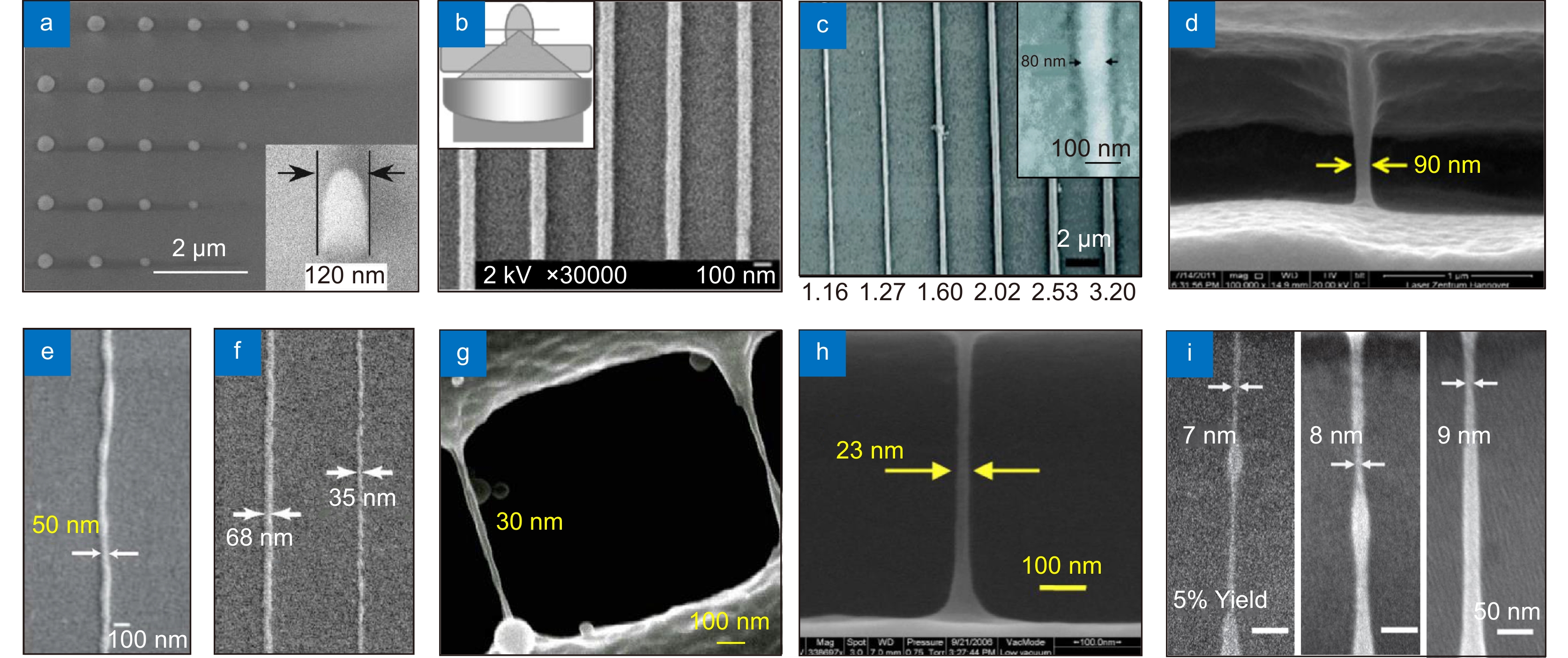
图 6 双光子聚合加工极限尺度纳米点、线结构。(a) 120 nm[19]、(b) 100 nm[98]、(c) 80 nm[100]、(d) 90 nm[101]、(e) 50 nm[103]、(f) 35 nm[74]、(g) 30 nm[104]、(h) 23 nm[105]、(i) 7 nm、8 nm和9 nm[106]特征尺度纳米点、线结构
Figure 6. The nanodots/wires structures fabricated by TPP.(a) 120 nm[19], (b) 100 nm[98], (c) 80 nm[100], (d) 90 nm[101], (e) 50 nm[103], (f) 35 nm[74], (g) 30 nm[104], (h) 23 nm[105], (i) 7 nm, 8 nm and 9 nm[106] feature size in the nanodots/wires structures
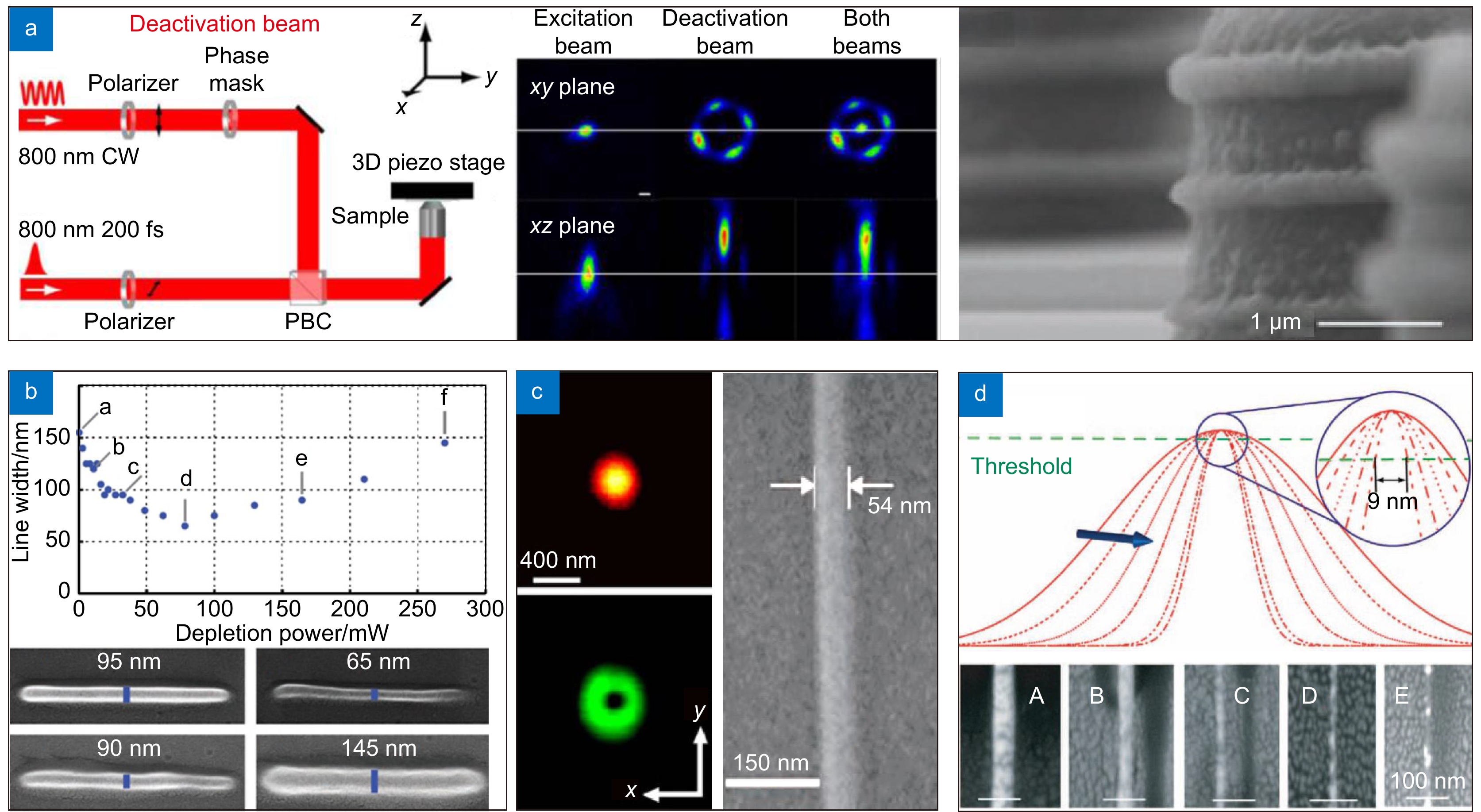
图 7 基于STED双光子聚合加工极限尺度纳米线结构。(a) 基于STED双光子加工示意图及制备的结构最小纵向尺寸40 nm[110];(b) 纳米线线宽与532 nm 连续激光抑制光束功率的关系图及制备的95 nm、65 nm、90 nm和145 nm宽度的纳米线[111];(c) 聚合光束和抑制光束截面强度分布图,及制备的54 nm宽度纳米线[112];(d) 通过增加抑制光强提高分辨力的原理图及加工的9 nm特征尺度纳米线结构[113]
Figure 7. The nanowires structures fabricated by STED-TPP. (a) Schematic diagram of the STED-TPP and the minimum longitudinal size of 40 nm[110]; (b) The relationship between the line width and the 532 nm CW laser and the fabricated nanowires with widths of 95 nm, 65 nm, 90 nm, and 145 nm[111]; (c) Cross-sectional intensity distributions of the initiation and inhibition laser beam, and the fabricated nanowires with width of 54 nm[112]; (d) Schematic diagram of improving resolution by increasing inhibition intensity and the fabricated nanowires with the minimum size of 9 nm[113]
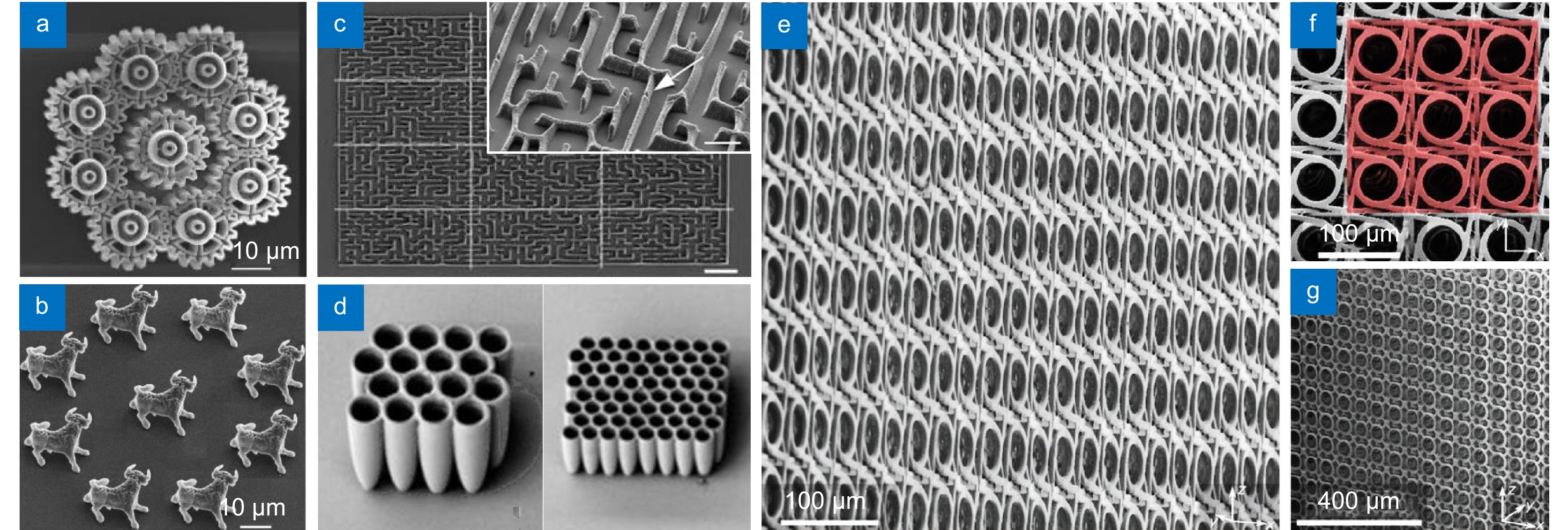
图 8 基于多光束并行加工制备的周期性三维结构。(a,b) 基于衍射元件直写加工的微齿轮和微米牛组合结构[120];(c) 基于DMD投影拼接的二维阵列结构[121];(d) 基于SLM直写加工的抛物面镜结构[122];(e-g) 基于衍射元件直写加工三维力学超材料[123]
Figure 8. Periodic 3D structures fabricated based on multi-beam parallel fabrication technology.(a,b) Micro-gear and micro-bull combined structures fabricated by TPP with diffractive elements[120]; (c) 2D array structure fabricated by TPP with DMD projection[121]; (d) Parabolic mirror structure based on SLM-TPP[122]; (e-g) 3D mechanical metamaterials fabricated by TPP with diffractive elements[123]
图 9 基于DMD双光子加工制备的高精度、大尺寸结构。(a) DMD全息多焦点3D双光子打印方法,及打印的高分辨“桥”结构,二元全息产生单焦点、双焦点、三焦点制备的木堆结构[125];(b) 基于DMD飞秒投影双光子光刻技术及制备的具有亚微米特征尺度的厘米级三维结构,微纳悬臂结构[126];(c) 基于时空聚焦DMD投影双光子光刻技术及制备的微纳悬线结构,宏观超材料结构[127];(d) 基于DMD飞秒面投影纳米光刻技术及制备的纳米线、点结构,跨尺度微纳结构[128]
Figure 9. High-precision, large-scale structures fabricated by DMD TPP technology.(a) DMD holographic multi-focus 3D TPP method and the fabricated high-resolution "bridge" structure, and woodpile structures[125]; (b) The prepared Millimeter-scale structure with sub-micrometer features, micro-nano bridge structures by FP-TPL technology[126]; (c) The prepared micro-nano suspended lines and micro-metamaterial structures by projection TPP with the spatiotemporal focusing technology[127]; (d) The prepared nanowires and nanodots structures, cross-scale structures by femtosecond projection nanolithography technology[128]
图 10 光子晶体、超材料与器件。(a) 木堆结构光子晶体[131];(b) 金刚石结构光子晶体[133];(c) 热收缩的木堆光子晶体[134];(d) 手性螺旋超材料[135];(e) 光波段的三维隐身衣结构[136];(f) 光束偏转器[137];(g) 复合手性光子晶体材料[138];(h) 圆偏振光分光器[139]
Figure 10. Photonic crystals, metamaterials, and devices. (a) Woodpile photonic crystal[131]; (b) Diamond photonic crystal[133]; (c) Heat shrinkable woodpile photonic crystal[134]; (d) Chiral helical metamaterial[135]; (e) 3D invisibility cloak structure in optical band[136]; (f) Beam deflector[137]; (g) Composite chiral photonic crystal material[138]; (h) Circularly polarized beam splitter[139]
图 11 超表面透镜器件。(a) 混合消色差超透镜宽带聚焦示意图[141];(b) 混合消色差超透镜的结构图[141];(c) 局部放大图[141];(d) 宽带近红外光成像效果[141];(e) 基于纳米孔相位板的宽带超透镜[142];(f) 测量的宽带聚焦光斑[142];(g) 可调焦距的 3D 双级联超透镜[146];(h) 测量的变焦距聚焦光斑[146]
Figure 11. Metalens device. (a) Schematic diagram of the broadband focusing of the hybrid achromatic metalens[141]; (b) The structure of the hybrid achromatic metalens[141]; (c) The partial enlarged view[141]; (d) The imaging of the broadband near-infrared light[141]; (e) The broadband metalens, which combines nanoholes with a phase plate[142]; (f) Measured broadband focusing spot[142]; (g) The tunable multifocal 3D metalens[146]; (h) Measured zoom focusing spot[146]

图 12 集成光子学器件。(a) 微型棱镜耦合器[148];(b) 低损耗光纤-片上耦合器[149];(c) 偏振旋转的聚合物矩形波导[150];(d) 光纤-片上连接器[153];(e) 芯片-芯片光连接器[153];(f) 片上器件-器件光连接器[153];(g) 微盘腔结构和光互联波导结构[154];(h) 三维弯曲表面光子微腔结构[155]
Figure 12. Integrated photonics device. (a) Miniature prism coupler[148]; (b) Low-loss fiber-on-chip coupler[149]; (c) Polarization-rotated polymer rectangular waveguide[150]; (d) Fiber-on-chip connector[153]; (e) Chip-on-chip optical connector[153]; (f) On-chip device-device optical connector[153]; (g) Microdisk cavity structure and optical interconnect waveguide structure[154]; (h) 3D curved surface photonic microcavity structure[155]
图 14 逆向设计微纳光学器件。(a) 自由形式近红外偏振分束器[163];(b) 光谱分离超表面透镜[164];(c) 3D圆对称超透镜[165];(d) 多层超透镜[166]
Figure 14. Inverse-designed micro-nano optics devices. (a) Free-form NIR polarizing beamsplitter[163]; (b) Spectral splitting metalens[164]; (c) 3D circularly symmetric metalens[165]; (d) Multilayer metalens[166]
图 15 力学超材料结构与器件。(a) 剪切模量消隐的五模式反膨胀力学超材料及上下两个直径不同相连接的双圆锥结构单元[168];(b) 无触感的弹性机械波斗篷[170];(c) 扭转机械超材料[171]
Figure 15. Mechanical metamaterial structures and devices.(a) Pentamode metamterials and structural unit of two connected truncated cones[168]; (b) An elasto-mechanical unfeelability cloak made of metamaterials[170]; (c) A twist mechanical metamaterials[171]
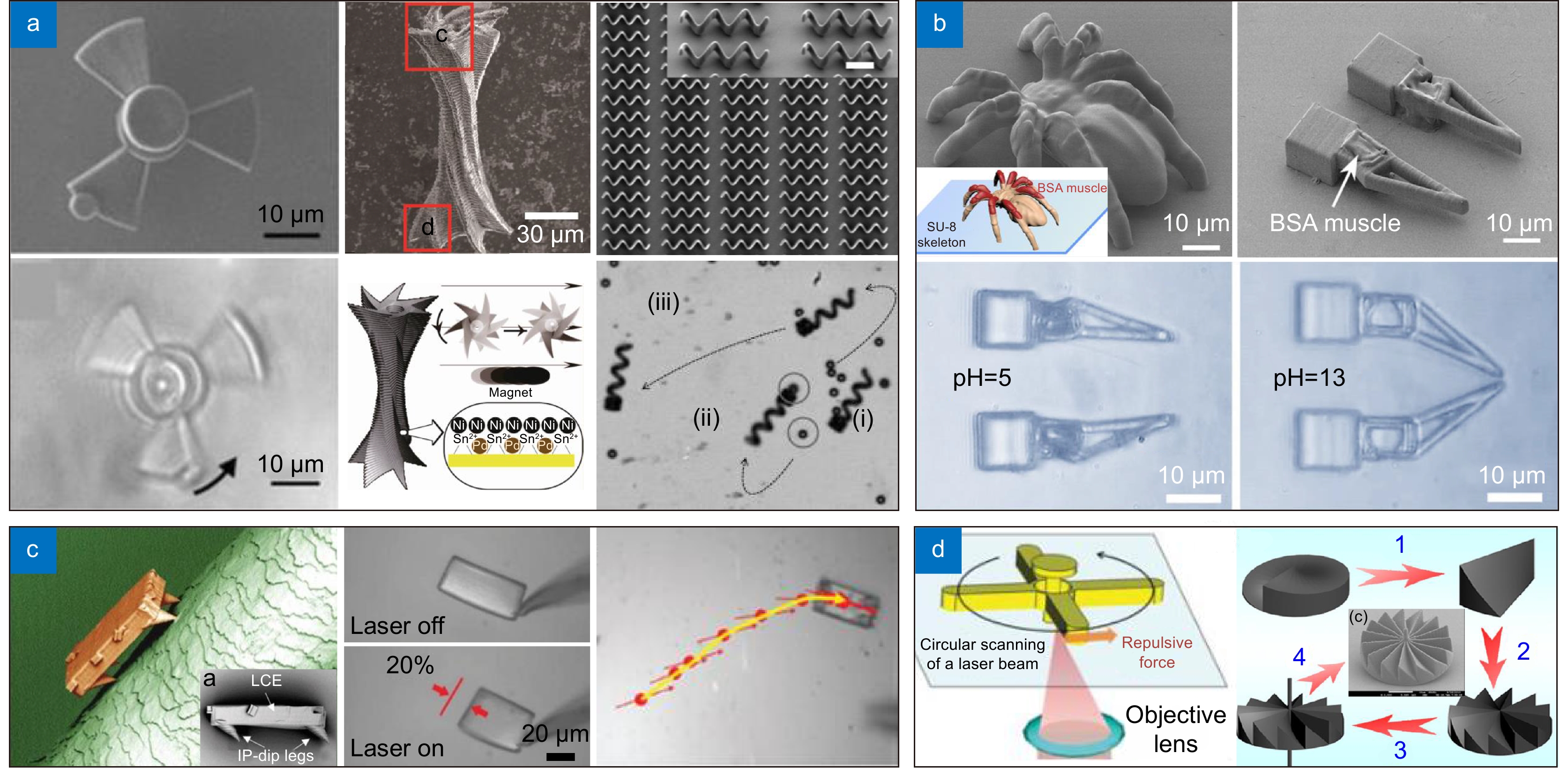
图 16 可驱动的微机械器件。(a) 可远程磁驱动的微型转子、微型盾构机和三维螺旋推进器[176];(b) pH响应蜘蛛微型机器人和智能微型抓手[179];(c) 基于液晶弹性体的微型步行者[180];(d) 基于光镊驱动的微机械转子[181-182]
Figure 16. Drivable micromechanical devices. (a) Remote magnetically actuated micro-rotor, micro-shield machine and 3D helical thruster[176]; (b) The pH-responsive spider micro-robot and smart micro-gripper[179]; (c) The liquid crystal elastomer-based micro-walker[180]; (d) Optical tweezers-driven micromechanical rotor[181-182]
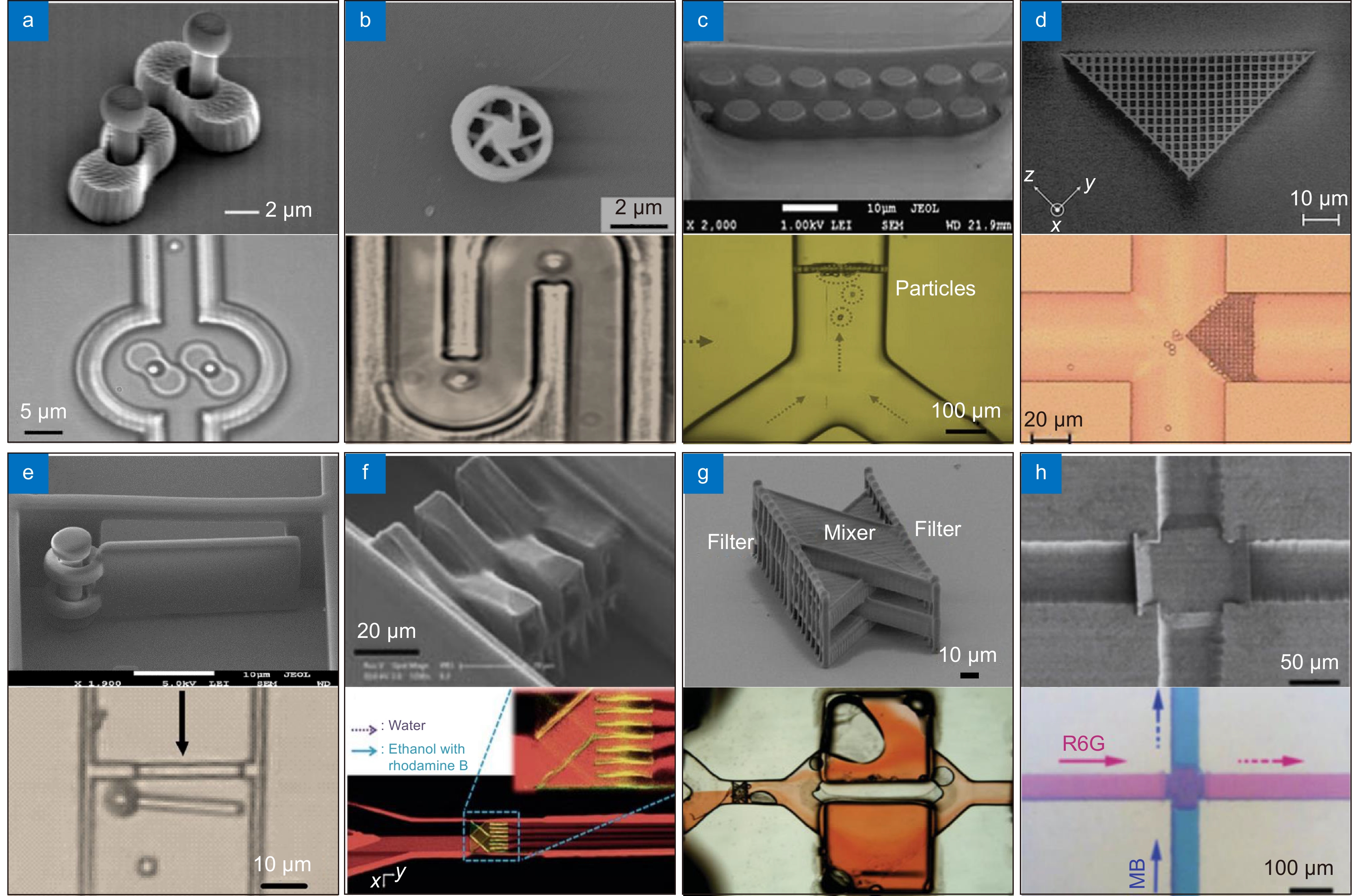
图 17 微流道器件。(a) 微泵[185];(b) 微涡轮[186];(c) 微筛[188];(d) 微过滤器[189];(e) 微阀门[190];(f) 微混合器[191];(g) 微混合器和过滤器[191];(d) 微立交桥器件[192]
Figure 17. Microfluidic device. (a) Micropump[185]; (b) Microturbines[186]; (c) Microsieves[188]; (d) Microfilters[189]; (e) Microvalve[190]; (f) Micromixer[191]; (g) Micromixer and filters[191]; (d) Micro-overpass devices[192]
聚合类型 自由基聚合 阳离子聚合 光解离 PI$ \begin{array}{*{20}{c}} {}&{\xrightarrow{{\begin{array}{*{20}{c}} 2 \hbar v \end{array}}}}&{}&{} \end{array} $PI* → R* PI$ \begin{array}{*{20}{c}} {}&{\xrightarrow{{\begin{array}{*{20}{c}} 2 \hbar v \end{array}}}}&{}&{} \end{array} $PI* → K+ 引发聚合 R* + M → RM* K+X− + M → KM+X− 链增长 RM* → RMM* → RMnR KM+X− + M → KMn+X− 链终止 Primary radical termination: RM* + R* → RMnRRecombination: RMn* + RMm* → RMn+mRDisproportionation: RMn* + RMm* → RMn+RMm Ionic rearrangement: KMn+X− → KMn + H+X−Chain transfer: KMn+X− + M → KMn + HM+X− 常见材料 (甲基)丙烯酸酯、乙烯基、硫醇、水凝胶、有机-无机杂化材料 主要是环氧树脂 商用光刻胶 SCR500, IP-L, IP-G, IP-Dip, SZ2080, PEG-DA,
PETA, OrmoComp, Ormocer, PDMSSU-8, SCR-701  下载: 导出CSV
-
[1] Pimpin A, Srituravanich W. Review on micro- and nanolithography techniques and their applications[J]. Eng J, 2012, 16(1): 37−56. doi: 10.4186/ej.2012.16.1.37
[2] Rothschild M. Projection optical lithography[J]. Mater Today, 2005, 8(2): 18−24. doi: 10.1016/S1369-7021(05)00698-X
[3] Fay B. Advanced optical lithography development, from UV to EUV[J]. Microelectron Eng, 2002, 61-62: 11−24. doi: 10.1016/S0167-9317(02)00427-6
[4] Silverman J P. Challenges and progress in x-ray lithography[J]. J Vac Sci Technol B Microelectron Nanometer Struct Process, Meas, Phenom, 1998, 16(6): 3137−3141. doi: 10.1116/1.590452
[5] Vieu C, Carcenac F, Pépin A, et al. Electron beam lithography: resolution limits and applications[J]. Appl Surf Sci, 2000, 164(1-4): 111−117. doi: 10.1016/S0169-4332(00)00352-4
[6] Manfrinato V R, Zhang L H, Su D, et al. Resolution limits of electron-beam lithography toward the atomic scale[J]. Nano Lett, 2013, 13(4): 1555−1558. doi: 10.1021/nl304715p
[7] Watt F, Bettiol A A, Van Kan J A, et al. Ion beam lithography and nanofabrication: a review[J]. Int J Nanosci, 2005, 4(3): 269−286. doi: 10.1142/S0219581X05003139
[8] Guo L J. Nanoimprint lithography: methods and material requirements[J]. Adv Mater, 2007, 19(4): 495−513. doi: 10.1002/adma.200600882
[9] Cox L M, Martinez A M, Blevins A K, et al. Nanoimprint lithography: emergent materials and methods of actuation[J]. Nano Today, 2020, 31: 100838. doi: 10.1016/j.nantod.2019.100838
[10] Pan D Z. Directed self-assembly for advanced chips[J]. Nat Electron, 2018, 1(10): 530−531. doi: 10.1038/s41928-018-0152-7
[11] 董贤子, 陈卫强, 赵震声, 等. 飞秒脉冲激光双光子微纳加工技术及其应用[J]. 科学通报, 2008, 53(1): 2−13. doi: 10.3321/j.issn:0023-074X.2008.01.002
Dong X Z, Chen W Q, Zhao Z S, et al. Femtosecond laser two-photon micro-/nano-fabrication and its applications[J]. Chin Sci Bull, 2008, 53(1): 2−13. doi: 10.3321/j.issn:0023-074X.2008.01.002
[12] 孙树峰, 王萍萍. 飞秒激光双光子聚合加工微纳结构[J]. 红外与激光工程, 2018, 47(12): 1206009. doi: 10.3788/IRLA201847.1206009
Sun S F, Wang P P. Micro/nano structures fabricated by two-photon photopolymerization of femtosecond laser[J]. Infrared Laser Eng, 2018, 47(12): 1206009. doi: 10.3788/IRLA201847.1206009
[13] Zhang Y L, Chen Q D, Xia H, et al. Designable 3D nanofabrication by femtosecond laser direct writing[J]. Nano Today, 2010, 5(5): 435−448. doi: 10.1016/j.nantod.2010.08.007
[14] Fourkas J T. Nanoscale photolithography with visible light[J]. J Phys Chem Lett, 2010, 1(8): 1221−1227. doi: 10.1021/jz1002082
[15] 赵圆圆. 微尺度结构的功能化及其集成制备技术研究[D]. 北京: 中国科学院大学, 2016.
Zhao Y Y. Research on functionalization of microscale structures and their integrated fabrication technology[D]. Beijing: University of Chinese Academy of Sciences, 2016
[16] 郑美玲, 金峰, 董贤子, 等. 双光子光聚合与功能微纳结构制备[J]. 影像科学与光化学, 2017, 35(4): 413−428. doi: 10.7517/j.issn.1674-0475.2017.04.006
Zheng M L, Jin F, Dong X Z, et al. Two-photon photopolymerization and functional micro/nanostructure fabrication[J]. Imag Sci Photochem, 2017, 35(4): 413−428. doi: 10.7517/j.issn.1674-0475.2017.04.006
[17] Hohmann J K, Renner M, Waller E H, et al. Three-dimensional μ-printing: an enabling technology[J]. Adv Opt Mater, 2015, 3(11): 1488−1507. doi: 10.1002/adom.201500328
[18] Maruo S, Nakamura O, Kawata S. Three-dimensional microfabrication with two-photon-absorbed photopolymerization[J]. Opt Lett, 1997, 22(2): 132−134. doi: 10.1364/OL.22.000132
[19] Kawata S, Sun H B, Tanaka T, et al. Finer features for functional microdevices[J]. Nature, 2001, 412(6848): 697−698. doi: 10.1038/35089130
[20] Li L J, Fourkas J T. Multiphoton polymerization[J]. Mater Today, 2007, 10(6): 30−37. doi: 10.1016/S1369-7021(07)70130-X
[21] Lu W E, Dong X Z, Chen W Q, et al. Novel photoinitiator with a radical quenching moiety for confining radical diffusion in two-photon induced photopolymerization[J]. J Mater Chem, 2011, 21(15): 5650−5659. doi: 10.1039/c0jm04025h
[22] Layani M, Wang X F, Magdassi S. Novel materials for 3D printing by photopolymerization[J]. Adv Mater, 2018, 30(41): 1706344. doi: 10.1002/adma.201706344
[23] Arnoux C, Konishi T, Van Elslande E, et al. Polymerization photoinitiators with near-resonance enhanced two-photon absorption cross-Section: toward high-resolution photoresist with improved sensitivity[J]. Macromolecules, 2020, 53(21): 9264−9278. doi: 10.1021/acs.macromol.0c01518
[24] Cônsoli P M, Otuka A J G, Balogh D T, et al. Feature size reduction in two‐photon polymerization by optimizing resin composition[J]. J Polym Sci Part B Polym Phys, 2018, 56(16): 1158−1163. doi: 10.1002/polb.24635
[25] Malinauskas M, Žukauskas A, Bičkauskaitė G, et al. Mechanisms of three-dimensional structuring of photo-polymers by tightly focussed femtosecond laser pulses[J]. Opt Express, 2010, 18(10): 10209−10221. doi: 10.1364/OE.18.010209
[26] Jeong H Y, Lee E, An S C, et al. 3D and 4D printing for optics and metaphotonics[J]. Nanophotonics, 2020, 9(5): 1139−1160. doi: 10.1515/nanoph-2019-0483
[27] Xiong C, Liao C R, Li Z Y, et al. Optical fiber integrated functional micro-/nanostructure induced by two-Photon polymerization[J]. Front Mater, 2020, 7: 586496. doi: 10.3389/fmats.2020.586496
[28] Koo S. Advanced micro-actuator/robot fabrication using ultrafast laser direct writing and its remote control[J]. Appl Sci, 2020, 10(23): 8563. doi: 10.3390/app10238563
[29] Harinarayana V, Shin Y C. Two-photon lithography for three-dimensional fabrication in micro/nanoscale regime: a comprehensive review[J]. Opt Laser Technol, 2021, 142: 107180. doi: 10.1016/j.optlastec.2021.107180
[30] Otuka A J G, Tomazio N B, Paula K T, et al. Two-photon polymerization: functionalized microstructures, micro-resonators, and bio-scaffolds[J]. Polymers, 2021, 13(12): 1994. doi: 10.3390/polym13121994
[31] Göppert-Mayer M. Elementary processes with two quantum transitions[J]. Ann Phys, 2009, 521(7-8): 466−479. doi: 10.1002/andp.200952107-804
[32] Kaiser W, Garrett C G B. Two-photon excitation in CaF2: Eu2+[J]. Phys Rev Lett, 1961, 7(6): 229−231. doi: 10.1103/PhysRevLett.7.229
[33] Wloka T, Gottschaldt M, Schubert U S. From light to structure: photo initiators for radical two‐photon polymerization[J]. Chem–Eur J, 2022, 28(32): e202104191. doi: 10.1002/chem.202104191
[34] Mukherjee A. Two-photon pumped upconverted lasing in dye doped polymer waveguides[J]. Appl Phys Lett, 1993, 62(26): 3423−3425. doi: 10.1063/1.109036
[35] Watanabe M, Juodkazis S, Sun H B, et al. Two-photon readout of three-dimensional memory in silica[J]. Appl Phys Lett, 2000, 77(1): 13−15. doi: 10.1063/1.126861
[36] Yamasaki K, Juodkazis S, Watanabe M, et al. Recording by microexplosion and two-photon reading of three-dimensional optical memory in polymethylmethacrylate films[J]. Appl Phys Lett, 2000, 76(8): 1000−1002. doi: 10.1063/1.125919
[37] Kirkpatrick S M, Baur J W, Clark C M, et al. Holographic recording using two-photon-induced photopolymerization[J]. Appl Phys A, 1999, 69(4): 461−464. doi: 10.1007/s003390051033
[38] Strickler J H, Webb W W. Three-dimensional optical data storage in refractive media by two-photon point excitation[J]. Opt Lett, 1991, 16(22): 1780−1782. doi: 10.1364/OL.16.001780
[39] Sun H B, Tanaka T, Takada K, et al. Two-photon photopolymerization and diagnosis of three-dimensional microstructures containing fluorescent dyes[J]. Appl Phys Lett, 2001, 79(10): 1411−1413. doi: 10.1063/1.1399312
[40] Diaspro A, Robello M. Two-photon excitation of fluorescence for three-dimensional optical imaging of biological structures[J]. J Photochem Photobiol B Biol, 2000, 55(1): 1−8. doi: 10.1016/S1011-1344(00)00028-2
[41] Kuebler S M, Rumi M, Watanabe T, et al. Optimizing two-photon initiators and exposure conditions for three-dimensional lithographic microfabrication[J]. J Photopolym Sci Technol, 2001, 14(4): 657−668. doi: 10.2494/photopolymer.14.657
[42] Sun H B, Kawata S. Two-photon laser precision microfabrication and its applications to micro-nano devices and systems[J]. J Lightw Technol, 2003, 21(3): 624−633. doi: 10.1109/JLT.2003.809564
[43] Liaros N, Fourkas J T. The characterization of absorptive nonlinearities[J]. Laser Photonics Rev, 2017, 11(5): 1700106. doi: 10.1002/lpor.201700106
[44] Liaros N, Fourkas J T. Methods for determining the effective order of absorption in radical multiphoton photoresists: a critical analysis[J]. Laser Photonics Rev, 2021, 15(1): 2000203. doi: 10.1002/lpor.202000203
[45] Baldacchini T. Three-Dimensional Microfabrication Using Two-Photon Polymerization: Fundamentals, Technology, and Applications[M]. Amsterdam: Elsevier, 2015.
[46] Skliutas E, Lebedevaite M, Kabouraki E, et al. Polymerization mechanisms initiated by spatio-temporally confined light[J]. Nanophotonics, 2021, 10(4): 1211−1242. doi: 10.1515/nanoph-2020-0551
[47] Bauhofer A. Multiscale effects of photochemical shrinkage in direct laser writing[D]. Zurich: ETH Zurich, 2019.
[48] Schafer K J, Hales J M, Balu M, et al. Two-photon absorption cross-sections of common photoinitiators[J]. J Photoch Photobio A Chem, 2004, 162(2-3): 497−502. doi: 10.1016/S1010-6030(03)00394-0
[49] Fischer J, Mueller J B, Kaschke J, et al. Three-dimensional multi-photon direct laser writing with variable repetition rate[J]. Opt Express, 2013, 21(22): 26244−26260. doi: 10.1364/OE.21.026244
[50] Parkatzidis K, Kabouraki E, Selimis A, et al. Initiator-free, multiphoton polymerization of gelatin methacrylamide[J]. Macromol Mater Eng, 2018, 303(12): 1800458. doi: 10.1002/mame.201800458
[51] Lebedevaite M, Ostrauskaite J, Skliutas E, et al. Photoinitiator free resins composed of plant-derived monomers for the optical µ-3D printing of thermosets[J]. Polymers, 2019, 11(1): 116. doi: 10.3390/polym11010116
[52] Stuart B C, Feit M D, Herman S, et al. Nanosecond-to-femtosecond laser-induced breakdown in dielectrics[J]. Phy Rev B, 1996, 53(4): 1749−1761. doi: 10.1103/PhysRevB.53.1749
[53] Hankin S M, Villeneuve D M, Corkum P B, et al. Nonlinear ionization of organic molecules in high intensity laser fields[J]. Phys Rev Lett, 2000, 84(22): 5082−5085. doi: 10.1103/PhysRevLett.84.5082
[54] 马文超, 邱迎昕. 基于光聚合技术的3D打印材料及未来发展方向[J]. 广东化工, 2019, 46(10): 91−92. doi: 10.3969/j.issn.1007-1865.2019.10.038
Ma W C, Qiu Y X. Mechanisms and future direction of 3D printing using photopolymerization[J]. Guangdong Chem Ind, 2019, 46(10): 91−92. doi: 10.3969/j.issn.1007-1865.2019.10.038
[55] Kiefer P, Hahn V, Nardi M, et al. Sensitive photoresists for rapid multiphoton 3D laser micro-and nanoprinting[J]. Adv Opt Mater, 2020, 8(19): 2000895. doi: 10.1002/adom.202000895
[56] Carlotti M, Mattoli V. Functional materials for two‐photon polymerization in microfabrication[J]. Small, 2019, 15(40): 1902687. doi: 10.1002/smll.201902687
[57] Serbin J, Egbert A, Ostendorf A, et al. Femtosecond laser-induced two-photon polymerization of inorganic–organic hybrid materials for applications in photonics[J]. Opt Lett, 2003, 28(5): 301−303. doi: 10.1364/OL.28.000301
[58] Doğruyol Z, Arsu N, Doğruyol S K, et al. Producing critical exponents from gelation for various photoinitiator concentrations; a photo differential scanning calorimetric study[J]. Prog Org Coat, 2012, 74(1): 181−185. doi: 10.1016/j.porgcoat.2011.12.007
[59] Goodner M D, Bowman C N. Modeling primary radical termination and its effects on autoacceleration in photopolymerization kinetics[J]. Macromolecules, 1999, 32(20): 6552−6559. doi: 10.1021/ma9901947
[60] Williams C G, Malik A N, Kim T K, et al. Variable cytocompatibility of six cell lines with photoinitiators used for polymerizing hydrogels and cell encapsulation[J]. Biomaterials, 2005, 26(11): 1211−1218. doi: 10.1016/j.biomaterials.2004.04.024
[61] Winter H H, Chambon F. Analysis of linear viscoelasticity of a crosslinking polymer at the gel point[J]. J Rheol, 1986, 30(2): 367−382. doi: 10.1122/1.549853
[62] Friedrich C, Heymann L. Extension of a model for crosslinking polymer at the gel point[J]. J Rheol, 1988, 32(3): 235−241. doi: 10.1122/1.549971
[63] Schwärzle D, Hou X, Prucker O, et al. Polymer microstructures through two‐photon crosslinking[J]. Adv Mater, 2017, 29(39): 1703469. doi: 10.1002/adma.201703469
[64] Anseth K S, Bowman C N, Peppas N A. Polymerization kinetics and volume relaxation behavior of photopolymerized multifunctional monomers producing highly crosslinked networks[J]. J Polym Sci Part A Polym Chem, 1994, 32(1): 139−147. doi: 10.1002/pola.1994.080320116
[65] Decker C, Jenkins A D. Kinetic approach of oxygen inhibition in ultraviolet-and laser-induced polymerizations[J]. Macromolecules, 1985, 18(6): 1241−1244. doi: 10.1021/ma00148a034
[66] Cicha K, Li Z Q, Stadlmann K, et al. Evaluation of 3D structures fabricated with two-photon-photopolymerization by using FTIR spectroscopy[J]. J Appl Phys, 2011, 110(6): 064911. doi: 10.1063/1.3639304
[67] Jiang L J, Zhou Y S, Xiong W, et al. Two-photon polymerization: investigation of chemical and mechanical properties of resins using Raman microspectroscopy[J]. Opt Lett, 2014, 39(10): 3034−3037. doi: 10.1364/OL.39.003034
[68] Burmeister F, Steenhusen S, Houbertz R, et al. Materials and technologies for fabrication of three-dimensional microstructures with sub-100 nm feature sizes by two-photon polymerization[J]. J Laser Appl, 2012, 24(4): 042014. doi: 10.2351/1.4730807
[69] Tanaka T, Sun H B, Kawata S. Rapid sub-diffraction-limit laser micro/nanoprocessing in a threshold material system[J]. Appl Phys Lett, 2002, 80(2): 312−314. doi: 10.1063/1.1432450
[70] Odian G. Principles of Polymerization[M]. 4th ed. Hoboken: John Wiley & Sons, 2004.
[71] Yang L, Münchinger A, Kadic M, et al. On the schwarzschild effect in 3D two-photon laser lithography[J]. Adv Opt Mater, 2019, 7(22): 1901040. doi: 10.1002/adom.201901040
[72] Muller J B. Exploring the mechanisms of Three-Dimensional direct laser writing by multi-photon polymerization[D]. Karlsruhe: Karlsruher Institut für Technologie, 2015.
[73] Wang S H, Yu Y, Liu H L, et al. Sub-10-nm suspended nano-web formation by direct laser writing[J]. Nano Futures, 2018, 2(2): 025006. doi: 10.1088/2399-1984/aabb94
[74] 宋旸, 董贤子, 赵震声, 等. 飞秒激光双光子加工的极限分辨力[J]. 强激光与粒子束, 2011, 23(7): 1780−1784. doi: 10.3788/HPLPB20112307.1780
Song Y, Dong X Z, Zhao Z S, et al. Investigation into ultimate resolution by femtosecond laser two-photon fabrication technique[J]. High Power Laser Part Beams, 2011, 23(7): 1780−1784. doi: 10.3788/HPLPB20112307.1780
[75] 张心正, 夏峰, 许京军. 激光超衍射加工机理与研究进展[J]. 物理学报, 2017, 66(4): 144207. doi: 10.7498/aps.66.144207
Zhang X Z, Xia F, Xu J J. The mechanisms and research progress of laser fabrication technologies beyond diffraction limit[J]. Acta Phys Sin, 2017, 66(4): 144207. doi: 10.7498/aps.66.144207
[76] Zhou X Q, Hou Y H, Lin J Q. A review on the processing accuracy of two-photon polymerization[J]. AIP Adv, 2015, 5(3): 030701. doi: 10.1063/1.4916886
[77] Fischer J. Three-dimensional optical lithography beyond the diffraction limit[D]. Verlag Nicht Ermittelbar, 2012.
[78] Adão R M R, Alves T L, Maibohm C, et al. Two-photon polymerization simulation and fabrication of 3D microprinted suspended waveguides for on-chip optical interconnects[J]. Opt Express, 2022, 30(6): 9623−9642. doi: 10.1364/OE.449641
[79] Pikulin A, Bityurin N. Spatial resolution in polymerization of sample features at nanoscale[J]. Phys Rev B, 2007, 75(19): 195430. doi: 10.1103/PhysRevB.75.195430
[80] Li W, Cao T X, Zhai Z H, et al. Influence of evanescent waves on the voxel profile in multipulse multiphoton polymerization nanofabrication[J]. Nanotechnology, 2013, 24(21): 215301. doi: 10.1088/0957-4484/24/21/215301
[81] He Z Q, Lee Y H, Gou F W, et al. Polarization-independent phase modulators enabled by two-photon polymerization[J]. Opt Express, 2017, 25(26): 33688−33694. doi: 10.1364/OE.25.033688
[82] Zandrini T, Liaros N, Jiang L J, et al. Effect of the resin viscosity on the writing properties of two-photon polymerization[J]. Opt Mater Express, 2019, 9(6): 2601−2616. doi: 10.1364/OME.9.002601
[83] Cao D Z, Ge G J, Wang K G. Two-photon subwavelength lithography with thermal light[J]. Appl Phys Lett, 2010, 97(5): 051105. doi: 10.1063/1.3472112
[84] Mueller J B, Fischer J, Mange Y J, et al. In-situ local temperature measurement during three-dimensional direct laser writing[J]. Appl Phys Lett, 2013, 103(12): 123107. doi: 10.1063/1.4821556
[85] Hu Z Y, Sun Y L, Hua J G, et al. Femtosecond laser nano-fabrication with extended processing range[J]. IEEE Photonics Technol Lett, 2019, 31(2): 133−136. doi: 10.1109/LPT.2018.2884568
[86] Obata K, El-Tamer A, Koch L, et al. High-aspect 3D two-photon polymerization structuring with widened objective working range (WOW-2PP)[J]. Light Sci Appl, 2013, 2(12): e116. doi: 10.1038/lsa.2013.72
[87] Chu W, Tan Y X, Wang P, et al. Centimeter‐height 3D printing with femtosecond laser two-photon polymerization[J]. Adv Mater Technol, 2018, 3(5): 1700396. doi: 10.1002/admt.201700396
[88] Klar T A, Wollhofen R, Jacak J. Sub-Abbe resolution: from STED microscopy to STED lithography[J]. Phys Scr, 2014, 2014(T162): 014049.
[89] Fischer J, Mueller J B, Quick A S, et al. Exploring the mechanisms in STED-enhanced direct laser writing[J]. Adv Opt Mater, 2015, 3(2): 221−232. doi: 10.1002/adom.201400413
[90] Cheng H, Golvari P, Xia C, et al. High-throughput microfabrication of axially tunable helices[J]. Photonics Res, 2022, 10(2): 303−315. doi: 10.1364/PRJ.439592
[91] Yang L, Qian D D, Xin C, et al. Two-photon polymerization of microstructures by a non-diffraction multifoci pattern generated from a superposed Bessel beam[J]. Opt Lett, 2017, 42(4): 743−746. doi: 10.1364/OL.42.000743
[92] Vizsnyiczai G, Kelemen L, Ormos P. Holographic multi-focus 3D two-photon polymerization with real-time calculated holograms[J]. Opt Express, 2014, 22(20): 24217−24223. doi: 10.1364/OE.22.024217
[93] Manousidaki M, Papazoglou D G, Farsari M, et al. 3D holographic light shaping for advanced multiphoton polymerization[J]. Opt Lett, 2020, 45(1): 85−88. doi: 10.1364/OL.45.000085
[94] Jenness N J, Wulff K D, Johannes M S, et al. Three-dimensional parallel holographic micropatterning using a spatial light modulator[J]. Opt Express, 2008, 16(20): 15942−15948. doi: 10.1364/OE.16.015942
[95] Lin H, Jia B H, Gu M. Dynamic generation of Debye diffraction-limited multifocal arrays for direct laser printing nanofabrication[J]. Opt Lett, 2011, 36(3): 406−408. doi: 10.1364/OL.36.000406
[96] Obata K, Koch J, Hinze U, et al. Multi-focus two-photon polymerization technique based on individually controlled phase modulation[J]. Opt Express, 2010, 18(16): 17193−17200. doi: 10.1364/OE.18.017193
[97] Sun H B, Tanaka T, Kawata S. Three-dimensional focal spots related to two-photon excitation[J]. Appl Phys Lett, 2002, 80(20): 3673−3675. doi: 10.1063/1.1478128
[98] Takada K, Sun H B, Kawata S. Improved spatial resolution and surface roughness in photopolymerization-based laser nanowriting[J]. Appl Phys Lett, 2005, 86(7): 071122. doi: 10.1063/1.1864249
[99] Takada K, Sun H B, Kawata S. The study on spatial resolution in two-photon induced polymerization[J]. Proc SPIE, 2006, 6110: 61100A.
[100] Xing J F, Dong X Z, Chen W Q, et al. Improving spatial resolution of two-photon microfabrication by using photoinitiator with high initiating efficiency[J]. Appl Phys Lett, 2007, 90(13): 131106. doi: 10.1063/1.2717532
[101] Emons M, Obata K, Binhammer T, et al. Two-photon polymerization technique with sub-50 nm resolution by sub-10 fs laser pulses[J]. Opt Mater Express, 2012, 2(7): 942−947. doi: 10.1364/OME.2.000942
[102] Haske W, Chen V W, Hales J M, et al. 65 nm feature sizes using visible wavelength 3-D multiphoton lithography[J]. Opt Express, 2007, 15(6): 3426−3436. doi: 10.1364/OE.15.003426
[103] Dong X Z, Zhao Z S, Duan X M. Improving spatial resolution and reducing aspect ratio in multiphoton polymerization nanofabrication[J]. Appl Phys Lett, 2008, 92(9): 091113. doi: 10.1063/1.2841042
[104] Juodkazis S, Mizeikis V, Seet K K, et al. Two-photon lithography of nanorods in SU-8 photoresist[J]. Nanotechnology, 2005, 16(6): 846−849. doi: 10.1088/0957-4484/16/6/039
[105] Tan D F, Li Y, Qi F J, et al. Reduction in feature size of two-photon polymerization using SCR500[J]. Appl Phys Lett, 2007, 90(7): 071106. doi: 10.1063/1.2535504
[106] Jin F, Liu J, Zhao Y Y, et al. λ/30 inorganic features achieved by multi-photon 3D lithography[J]. Nat Commun, 2022, 13(1): 1357. doi: 10.1038/s41467-022-29036-7
[107] Fischer J, Wegener M. Three-dimensional direct laser writing inspired by stimulated-emission-depletion microscopy [Invited][J]. Opt Mater Express, 2011, 1(4): 614−624. doi: 10.1364/OME.1.000614
[108] Fischer J, Wegener M. Three-dimensional optical laser lithography beyond the diffraction limit[J]. Laser Photonics Rev, 2013, 7(1): 22−44. doi: 10.1002/lpor.201100046
[109] 曹耀宇, 谢飞, 张鹏达, 等. 双光束超分辨激光直写纳米加工技术[J]. 光电工程, 2017, 44(12): 1133−1145. doi: 10.3969/j.issn.1003-501X.2017.12.001
Cao Y Y, Xie F, Zhang P D, et al. Dual-beam super-resolution direct laser writing nanofabrication technology[J]. Opto-Electron Eng, 2017, 44(12): 1133−1145. doi: 10.3969/j.issn.1003-501X.2017.12.001
[110] Li L J, Gattass R R, Gershgoren E, et al. Achieving λ/20 resolution by one-color initiation and deactivation of polymerization[J]. Science, 2009, 324(5929): 910−913. doi: 10.1126/science.1168996
[111] Fischer J, Von Freymann G, Wegener M. The materials challenge in diffraction-unlimited direct-laser-writing optical lithography[J]. Adv Mater, 2010, 22(32): 3578−3582. doi: 10.1002/adma.201000892
[112] Wollhofen R, Katzmann J, Hrelescu C, et al. 120 nm resolution and 55 nm structure size in STED-lithography[J]. Opt Express, 2013, 21(9): 10831−10840. doi: 10.1364/OE.21.010831
[113] Gan Z S, Cao Y Y, Evans R A, et al. Three-dimensional deep sub-diffraction optical beam lithography with 9 nm feature size[J]. Nat Commun, 2013, 4(1): 2061. doi: 10.1038/ncomms3061
[114] Park S H, Lee S H, Yang D Y, et al. Subregional slicing method to increase three-dimensional nanofabrication efficiency in two-photon polymerization[J]. Appl Phys Lett, 2005, 87(15): 154108. doi: 10.1063/1.2103393
[115] Yang H, Zhao Y Y, Zheng M L, et al. Stepwise optimized 3D printing of arbitrary 3D structures at millimeter scale with high precision surface[J]. Macromol Mater Eng, 2019, 304(11): 1900400. doi: 10.1002/mame.201900400
[116] Sun H B, Nakamura A, Shoji S, et al. Three-dimensional nanonetwork assembled in a photopolymerized rod array[J]. Adv Mater, 2003, 15(23): 2011−2014. doi: 10.1002/adma.200305285
[117] Kuroiwa Y, Takeshima N, Narita Y, et al. Arbitrary micropatterning method in femtosecond laser microprocessing using diffractive optical elements[J]. Opt Express, 2004, 12(9): 1908−1915. doi: 10.1364/OPEX.12.001908
[118] Kato J I, Takeyasu N, Adachi Y, et al. Multiple-spot parallel processing for laser micronanofabrication[J]. Appl Phys Lett, 2005, 86(4): 044102. doi: 10.1063/1.1855404
[119] Matsuo S, Juodkazis S, Misawa H. Femtosecond laser microfabrication of periodic structures using a microlens array[J]. Appl Phys A, 2005, 80(4): 683−685. doi: 10.1007/s00339-004-3108-x
[120] Dong X Z, Zhao Z S, Duan X M. Micronanofabrication of assembled three-dimensional microstructures by designable multiple beams multiphoton processing[J]. Appl Phys Lett, 2007, 91(12): 124103. doi: 10.1063/1.2789661
[121] Ritschdorff E T, Nielson R, Shear J B. Multi-focal multiphoton lithography[J]. Lab Chip, 2012, 12(5): 867−871. doi: 10.1039/c2lc21271d
[122] Yan W S, Cumming B P, Gu M. High-throughput fabrication of micrometer-sized compound parabolic mirror arrays by using parallel laser direct-write processing[J]. J Opt, 2015, 17(7): 075803. doi: 10.1088/2040-8978/17/7/075803
[123] Hahn V, Kiefer P, Frenzel T, et al. Rapid assembly of small materials building blocks (voxels) into large functional 3D metamaterials[J]. Adv Funct Mater, 2020, 30(26): 1907795. doi: 10.1002/adfm.201907795
[124] Lin W, Chen D H, Chen S C. Emerging micro-additive manufacturing technologies enabled by novel optical methods[J]. Photonics Res, 2020, 8(12): 1827−1842. doi: 10.1364/PRJ.404334
[125] Geng Q, Wang D E, Chen P F, et al. Ultrafast multi-focus 3-D nano-fabrication based on two-photon polymerization[J]. Nat Commun, 2019, 10(1): 2179. doi: 10.1038/s41467-019-10249-2
[126] Saha S K, Wang D E, Nguyen V H, et al. Scalable submicrometer additive manufacturing[J]. Science, 2019, 366(6461): 105−109. doi: 10.1126/science.aax8760
[127] Somers P, Liang Z H, Johnson J E, et al. Rapid, continuous projection multi-photon 3D printing enabled by spatiotemporal focusing of femtosecond pulses[J]. Light Sci Appl, 2021, 10(1): 199. doi: 10.1038/s41377-021-00645-z
[128] Liu Y H, Zhao Y Y, Jin F, et al. λ/12 super resolution achieved in maskless optical projection nanolithography for efficient cross-scale patterning[J]. Nano Lett, 2021, 21(9): 3915−3921. doi: 10.1021/acs.nanolett.1c00559
[129] Duan X M, Sun H B, Kaneko K, et al. Two-photon polymerization of metal ions doped acrylate monomers and oligomers for three-dimensional structure fabrication[J]. Thin Solid Films, 2004, 453-454: 518−521. doi: 10.1016/j.tsf.2003.11.126
[130] Wong S, Deubel M, Pérez-Willard F, et al. Direct laser writing of three-dimensional photonic crystals with a complete photonic bandgap in chalcogenide glasses[J]. Adv Mater, 2006, 18(3): 265−269. doi: 10.1002/adma.200501973
[131] Ledermann A, Cademartiri L, Hermatschweiler M, et al. Three-dimensional silicon inverse photonic quasicrystals for infrared wavelengths[J]. Nat Mater, 2006, 5(12): 942−945. doi: 10.1038/nmat1786
[132] Ya Q, Chen W Q, Dong X Z, et al. Dual photonic band gap and reversible tuning of 3D photonic crystal fabricated by multiphoton polymerization with photoresponsive polymer[J]. Appl Phys A, 2008, 93(2): 393−398. doi: 10.1007/s00339-008-4789-3
[133] Dong X Z, Ya Q, Sheng X Z, et al. Photonic bandgap of gradient quasidiamond lattice photonic crystal[J]. Appl Phys Lett, 2008, 92(23): 231103. doi: 10.1063/1.2943278
[134] Liu Y J, Wang H, Ho J, et al. Structural color three-dimensional printing by shrinking photonic crystals[J]. Nat Commun, 2019, 10(1): 4340. doi: 10.1038/s41467-019-12360-w
[135] Gansel J K, Thiel M, Rill M S, et al. Gold helix photonic metamaterial as broadband circular polarizer[J]. Science, 2009, 325(5947): 1513−1515. doi: 10.1126/science.1177031
[136] Ergin T, Stenger N, Brenner P, et al. Three-dimensional invisibility cloak at optical wavelengths[J]. Science, 2010, 328(5976): 337−339. doi: 10.1126/science.1186351
[137] Digaum J L, Pazos J J, Chiles J, et al. Tight control of light beams in photonic crystals with spatially-variant lattice orientation[J]. Opt Express, 2014, 22(21): 25788−25804. doi: 10.1364/OE.22.025788
[138] Turner M D, Schröder-Turk G E, Gu M. Fabrication and characterization of three-dimensional biomimetic chiral composites[J]. Opt Express, 2011, 19(10): 10001−10008. doi: 10.1364/OE.19.010001
[139] Turner M D, Saba M, Zhang Q M, et al. Miniature chiral beamsplitter based on gyroid photonic crystals[J]. Nat Photonics, 2013, 7(10): 801−805. doi: 10.1038/nphoton.2013.233
[140] Li H L, Lee W B, Zhou C Y, et al. Flat retroreflector based on a metasurface doublet enabling reliable and angle-tolerant free-space optical link[J]. Adv Opt Mater, 2021, 9(21): 2100796. doi: 10.1002/adom.202100796
[141] Balli F, Sultan M, Lami S K, et al. A hybrid achromatic metalens[J]. Nat Commun, 2020, 11(1): 3892. doi: 10.1038/s41467-020-17646-y
[142] Balli F, Sultan M A, Ozdemir A, et al. An ultrabroadband 3D achromatic metalens[J]. Nanophotonics, 2021, 10(4): 1259−1264. doi: 10.1515/nanoph-2020-0550
[143] McLamb M, Li Y Z, Stinson P, et al. Metasurfaces for the infrared spectral range fabricated using two-photon polymerization[J]. Thin Solid Films, 2021, 721: 138548. doi: 10.1016/j.tsf.2021.138548
[144] Arbabi A, Arbabi E, Kamali S M, et al. Miniature optical planar camera based on a wide-angle metasurface doublet corrected for monochromatic aberrations[J]. Nat Commun, 2016, 7(1): 13682. doi: 10.1038/ncomms13682
[145] Hu Z Y, Jiang T, Tian Z N, et al. Broad-bandwidth micro-diffractive optical elements[J]. Laser Photonics Rev, 2022, 16(3): 2100537. doi: 10.1002/lpor.202100537
[146] Balli F. Optical metasurfaces[D]. Lexington: University of Kentucky, 2021.
[147] Sultan M A, Balli F, Lau D L, et al. Hybrid metasurfaces for simultaneous focusing and filtering[J]. Opt Lett, 2021, 46(2): 214−217. doi: 10.1364/OL.410080
[148] Safronov K R, Bessonov V O, Akhremenkov D V, et al. Miniature otto prism coupler for integrated photonics[J]. Laser Photonics Rev, 2022, 16(4): 2100542. doi: 10.1002/lpor.202100542
[149] Gehring H, Blaicher M, Hartmann W, et al. Low-loss fiber-to-chip couplers with ultrawide optical bandwidth[J]. APL Photonics, 2019, 4(1): 010801. doi: 10.1063/1.5064401
[150] Hou Z S, Xiong X, Cao J J, et al. On-chip polarization rotators[J]. Adv Opt Mater, 2019, 7(10): 1900129. doi: 10.1002/adom.201900129
[151] Blaicher M, Billah M R, Kemal J, et al. Hybrid multi-chip assembly of optical communication engines by in situ 3D nano-lithography[J]. Light Sci Appl, 2020, 9(1): 71. doi: 10.1038/s41377-020-0272-5
[152] Schumann M, Bückmann T, Gruhler N, et al. Hybrid 2D–3D optical devices for integrated optics by direct laser writing[J]. Light Sci Appl, 2014, 3(6): e175. doi: 10.1038/lsa.2014.56
[153] Lindenmann N, Balthasar G, Hillerkuss D, et al. Photonic wire bonding: a novel concept for chip-scale interconnects[J]. Opt Express, 2012, 20(16): 17667−17677. doi: 10.1364/OE.20.017667
[154] Nocentini S, Riboli F, Burresi M, et al. Three-dimensional photonic circuits in rigid and soft polymers tunable by light[J]. ACS Photonics, 2018, 5(8): 3222−3230. doi: 10.1021/acsphotonics.8b00461
[155] Bekenstein R, Kabessa Y, Sharabi Y, et al. Control of light by curved space in nanophotonic structures[J]. Nat Photonics, 2017, 11(10): 664−670. doi: 10.1038/s41566-017-0008-0
[156] Keum D, Jang K W, Jeon D S, et al. Xenos peckii vision inspires an ultrathin digital camera[J]. Light Sci Appl, 2018, 7(1): 80. doi: 10.1038/s41377-018-0081-2
[157] Gissibl T, Thiele S, Herkommer A, et al. Two-photon direct laser writing of ultracompact multi-lens objectives[J]. Nat Photonics, 2016, 10(8): 554−560. doi: 10.1038/nphoton.2016.121
[158] Bogucki A, Zinkiewicz Ł, Grzeszczyk M, et al. Ultra-long-working-distance spectroscopy of single nanostructures with aspherical solid immersion microlenses[J]. Light Sci Appl, 2020, 9(1): 48. doi: 10.1038/s41377-020-0284-1
[159] Thiele S, Arzenbacher K, Gissibl T, et al. 3D-printed eagle eye: compound microlens system for foveated imaging[J]. Sci Adv, 2017, 3(2): e1602655. doi: 10.1126/sciadv.1602655
[160] Thiele S, Pruss C, Herkommer A M, et al. 3D printed stacked diffractive microlenses[J]. Opt Express, 2019, 27(24): 35621−35630. doi: 10.1364/OE.27.035621
[161] Zhao Y Y, Zhang Y L, Zheng M L, et al. Three-dimensional Luneburg lens at optical frequencies[J]. Laser Photonics Rev, 2016, 10(4): 665−672. doi: 10.1002/lpor.201600051
[162] Xia C, Gutierrez J J, Kuebler S M, et al. Cylindrical-lens-embedded photonic crystal based on self-collimation[J]. Opt Express, 2022, 30(6): 9165−9180. doi: 10.1364/OE.452467
[163] Wei H M, Callewaert F, Hadibrata W, et al. Two-photon direct laser writing of inverse-designed free-form near-infrared polarization beamsplitter[J]. Adv Opt Mater, 2019, 7(21): 1900513. doi: 10.1002/adom.201900513
[164] Camayd-Muñoz P, Faraon A. Scaling laws for inverse-designed metadevices[C]//CLEO: QELS_Fundamental Science 2018, 2018: FF3C. 7.
[165] Hadibrata W, Wei H M, Krishnaswamy S, et al. Inverse design and 3D printing of a metalens on an optical fiber tip for direct laser lithography[J]. Nano Lett, 2021, 21(6): 2422−2428. doi: 10.1021/acs.nanolett.0c04463
[166] Roques-Carmes C, Lin Z, Christiansen R E, et al. Toward 3D-printed inverse-designed metaoptics[J]. ACS Photonics, 2022, 9(1): 43−51. doi: 10.1021/acsphotonics.1c01442
[167] Surjadi J U, Gao L B, Du H F, et al. Mechanical metamaterials and their engineering applications[J]. Adv Eng Mater, 2019, 21(3): 1800864. doi: 10.1002/adem.201800864
[168] Kadic M, Bückmann T, Stenger N, et al. On the practicability of pentamode mechanical metamaterials[J]. Appl Phys Lett, 2012, 100(19): 191901. doi: 10.1063/1.4709436
[169] Kadic M, Bückmann T, Schittny R, et al. Pentamode metamaterials with independently tailored bulk modulus and mass density[J]. Phys Rev Appl, 2014, 2(5): 054007. doi: 10.1103/PhysRevApplied.2.054007
[170] Bückmann T, Thiel M, Kadic M, et al. An elasto-mechanical unfeelability cloak made of pentamode metamaterials[J]. Nat Commun, 2014, 5(1): 4130. doi: 10.1038/ncomms5130
[171] Frenzel T, Kadic M, Wegener M. Three-dimensional mechanical metamaterials with a twist[J]. Science, 2017, 358(6366): 1072−1074. doi: 10.1126/science.aao4640
[172] Williams G, Hunt M, Boehm B, et al. Two-photon lithography for 3D magnetic nanostructure fabrication[J]. Nano Res, 2018, 11(2): 845−854. doi: 10.1007/s12274-017-1694-0
[173] Lao Z X, Xia N, Wang S J, et al. Tethered and untethered 3D microactuators fabricated by two-photon polymerization: a review[J]. Micromachines, 2021, 12(4): 465. doi: 10.3390/mi12040465
[174] He Z Q, Tan G J, Chanda D, et al. Novel liquid crystal photonic devices enabled by two-photon polymerization [Invited][J]. Opt Express, 2019, 27(8): 11472−11491. doi: 10.1364/OE.27.011472
[175] Zheng C L, Jin F, Zhao Y Y, et al. Light-driven micron-scale 3D hydrogel actuator produced by two-photon polymerization microfabrication[J]. Sensor Actuat B Chem, 2020, 304: 127345. doi: 10.1016/j.snb.2019.127345
[176] Xia H, Wang J, Tian Y, et al. Ferrofluids for fabrication of remotely controllable micro-nanomachines by two-photon polymerization[J]. Adv Mater, 2010, 22(29): 3204−3207. doi: 10.1002/adma.201000542
[177] Wang W K, Sun Z B, Zheng M L, et al. Magnetic nickel–phosphorus/polymer composite and remotely driven three-dimensional micromachine fabricated by nanoplating and two-photon polymerization[J]. J Phys Chem C, 2011, 115(22): 11275−11281. doi: 10.1021/jp202644d
[178] Tottori S, Zhang L, Qiu F M, et al. Magnetic helical micromachines: fabrication, controlled swimming, and cargo transport[J]. Adv Mater, 2012, 24(6): 811−816. doi: 10.1002/adma.201103818
[179] Ma Z C, Zhang Y L, Han B, et al. Femtosecond laser programmed artificial musculoskeletal systems[J]. Nat Commun, 2020, 11(1): 4536. doi: 10.1038/s41467-020-18117-0
[180] Zeng H, Wasylczyk P, Parmeggiani C, et al. Light-fueled microscopic walkers[J]. Adv Mater, 2015, 27(26): 3883−3887. doi: 10.1002/adma.201501446
[181] Lin X F, Hu G Q, Chen Q D, et al. A light-driven turbine-like micro-rotor and study on its light-to-mechanical power conversion efficiency[J]. Appl Phys Lett, 2012, 101(11): 113901. doi: 10.1063/1.4751464
[182] Ikegami T, Ozawa R, Stocker M P, et al. Development of optically-driven metallic microrotors using two-photon microfabrication[J]. J Laser Micro Nanoen, 2013, 8(1): 6−10. doi: 10.2961/jlmn.2013.01.0002
[183] Zhou W H, Kuebler S M, Braun K L, et al. An efficient two-photon-generated photoacid applied to positive-tone 3D microfabrication[J]. Science, 2002, 296(5570): 1106−1109. doi: 10.1126/science.296.5570.1106
[184] Baldacchini T. Three-Dimensional Microfabrication Using Two-Photon Polymerization[M]. 2nd ed. Oxford: William Andrew, 2019.
[185] Maruo S, Inoue H. Optically driven micropump produced by three-dimensional two-photon microfabrication[J]. Appl Phys Lett, 2006, 89(14): 144101. doi: 10.1063/1.2358820
[186] Maruo S, Takaura A, Saito Y. Optically driven micropump with a twin spiral microrotor[J]. Opt Express, 2009, 17(21): 18525−18532. doi: 10.1364/OE.17.018525
[187] Wang J, He Y, Xia H, et al. Embellishment of microfluidic devices via femtosecond laser micronanofabrication for chip functionalization[J]. Lab Chip, 2010, 10(15): 1993−1996. doi: 10.1039/c003264f
[188] Amato L, Gu Y, Bellini N, et al. Integrated three-dimensional filter separates nanoscale from microscale elements in a microfluidic chip[J]. Lab Chip, 2012, 12(6): 1135−1142. doi: 10.1039/c2lc21116e
[189] Wu D, Chen Q D, Niu L G, et al. Femtosecond laser rapid prototyping of nanoshells and suspending components towards microfluidic devices[J]. Lab Chip, 2009, 9(16): 2391−2394. doi: 10.1039/b902159k
[190] Lim T W, Son Y, Jeong Y J, et al. Three-dimensionally crossing manifold micro-mixer for fast mixing in a short channel length[J]. Lab Chip, 2011, 11(1): 100−103. doi: 10.1039/C005325M
[191] Wu D, Wu S Z, Xu J, et al. Hybrid femtosecond laser microfabrication to achieve true 3D glass/polymer composite biochips with multiscale features and high performance: the concept of ship-in-a-bottle biochip[J]. Laser Photonics Rev, 2014, 8(3): 458−467. doi: 10.1002/lpor.201400005
[192] He Y, Huang B L, Lu D X, et al. “Overpass” at the junction of a crossed microchannel: An enabler for 3D microfluidic chips[J]. Lab Chip, 2012, 12(20): 3866−3869. doi: 10.1039/c2lc40401j
[193] Hahn V, Messer T, Bojanowski N M, et al. Two-step absorption instead of two-photon absorption in 3D nanoprinting[J]. Nat Photonics, 2021, 15(12): 932−938. doi: 10.1038/s41566-021-00906-8
[194] Ueno K, Juodkazis S, Shibuya T, et al. Nanoparticle plasmon-assisted two-photon polymerization induced by incoherent excitation source[J]. J Am Chem Soc, 2008, 130(22): 6928−6929. doi: 10.1021/ja801262r
[195] Thiel M, Fischer J, Von Freymann G, et al. Direct laser writing of three-dimensional submicron structures using a continuous-wave laser at 532 nm[J]. Appl Phys Lett, 2010, 97(22): 221102. doi: 10.1063/1.3521464
[196] Mueller P, Thiel M, Wegener M. 3D direct laser writing using a 405 nm diode laser[J]. Opt Lett, 2014, 39(24): 6847−6850. doi: 10.1364/OL.39.006847
[197] Yu H Y, Ding H B, Zhang Q M, et al. Three-dimensional direct laser writing of PEGda hydrogel microstructures with low threshold power using a green laser beam[J]. Light Adv Manuf, 2021, 2(1): 31−38. doi: 10.37188/lam.2021.003
[198] Gräfe D, Wickberg A, Zieger M M, et al. Adding chemically selective subtraction to multi-material 3D additive manufacturing[J]. Nat Commun, 2018, 9(1): 2788. doi: 10.1038/s41467-018-05234-0
[199] Fang G, Cao H Z, Cao L C, et al. Femtosecond laser direct writing of 3D silica-like microstructure from hybrid epoxy cyclohexyl POSS[J]. Adv Mater Technol, 2018, 3(3): 1700271. doi: 10.1002/admt.201700271
[200] Hirt L, Reiser A, Spolenak R, et al. Additive manufacturing of metal structures at the micrometer scale[J]. Adv Mater, 2017, 29(17): 1604211. doi: 10.1002/adma.201604211
[201] Ma Z C, Zhang Y L, Han B, et al. Femtosecond-laser direct writing of metallic micro/nanostructures: from fabrication strategies to future applications[J]. Small Methods, 2018, 2(7): 1700413. doi: 10.1002/smtd.201700413
[202] Cao Y Y, Takeyasu N, Tanaka T, et al. 3D metallic nanostructure fabrication by surfactant-assisted multiphoton-induced reduction[J]. Small, 2009, 5(10): 1144−1148. doi: 10.1002/smll.200801179
[203] Zhao Y Y, Ren X L, Zheng M L, et al. Plasmon-enhanced nanosoldering of silver nanoparticles for high-conductive nanowires electrodes[J]. Opto-Electron Adv, 2021, 4(12): 200101. doi: 10.29026/oea.2021.200101
[204] 周伟平, 白石, 谢祖武, 等. 激光直写制备金属与碳材料微纳结构与器件研究进展[J]. 光电工程, 2022, 49(1): 210330. doi: 10.12086/oee.2022.210330
Zhou W P, Bai S, Xie Z W, et al. Research progress of laser direct writing fabrication of metal and carbon micro/nano structures and devices[J]. Opto-Electron Eng, 2022, 49(1): 210330. doi: 10.12086/oee.2022.210330
[205] Merkininkaitė G, Aleksandravičius E, Malinauskas M, et al. Laser additive manufacturing of Si/ZrO2 tunable crystalline phase 3D nanostructures[J]. Opto-Electron Adv, 2022, 5(5): 210077. doi: 10.29026/oea.2022.210077
[206] Li Y, Chen L W, Kong F, et al. Functional micro-concrete 3D hybrid structures fabricated by two-photon polymerization[J]. Opto-Electron Eng, 2017, 44(4): 393−399.
[207] Kotz F, Quick A S, Risch P, et al. Two-photon polymerization of nanocomposites for the fabrication of transparent fused silica glass microstructures[J]. Adv Mater, 2021, 33(9): 2006341. doi: 10.1002/adma.202006341
[208] Doualle T, André J C, Gallais L. 3D printing of silica glass through a multiphoton polymerization process[J]. Opt Lett, 2021, 46(2): 364−367. doi: 10.1364/OL.414848
[209] Wen X W, Zhang B Y, Wang W P, et al. 3D-printed silica with nanoscale resolution[J]. Nat Mater, 2021, 20(11): 1506−1511. doi: 10.1038/s41563-021-01111-2
[210] Ocier C R, Richards C A, Bacon-Brown D A, et al. Direct laser writing of volumetric gradient index lenses and waveguides[J]. Light Sci Appl, 2020, 9(1): 196. doi: 10.1038/s41377-020-00431-3
[211] Dottermusch S, Busko D, Langenhorst M, et al. Exposure-dependent refractive index of Nanoscribe IP-Dip photoresist layers[J]. Opt Lett, 2019, 44(1): 29−32. doi: 10.1364/OL.44.000029
-
 点击扫一扫
点击扫一扫
图(18)
表(1)
计量
- 文章访问数: 14110
- PDF下载数: 2003
- 施引文献: 0


