-
摘要
作为三维超构材料的衍生物,具有亚波长厚度的人工超构表面结构能够在紧凑的平台上灵活操纵光与物质的相互作用,有利于多功能、超紧凑光子器件的研发,对于微纳光子学和集成光子学具有重要意义。铁电晶体铌酸锂凭借其跨越可见光至中红外波段的宽透明窗口以及较大的非线性光学、电光系数,被认为是最有前途的多功能集成光子平台之一。近年来,基于铌酸锂薄膜(lithium-niobate-on-insulator,LNOI)的集成光子学器件研究也得到了迅猛发展。本文总结了几种有潜力制备高质量铌酸锂超构表面的微纳加工技术,同时介绍了近年来铌酸锂超构表面结构的研究进展,并对其未来的研究方向进行了展望。
Abstract
As derivatives of 3D metamaterials, artificial metasurface structures with sub-wavelength thicknesses can flexibly manipulate light-matter interactions in a compact manner, which is beneficial for the fabrication of multi-functional and ultracompact photonic devices. Therefore, metasurface structures are of great significance for micro-nano photonics and integrated photonics. The ferroelectric crystal lithium niobate is regarded as one of the most promising multifunctional integrated photonic platforms due to its wide transparent window spanning from the visible to the mid-infrared band as well as large nonlinear optical and electro-optic coefficients. In recent years, research on integrated photonics devices based on lithium-niobate-on-insulator (LNOI) thin films has also been developed rapidly. In this paper, several micro-nano processing technologies that have the potential to prepare high-quality lithium niobate metasurfaces are summarized. At the same time, the research progress of lithium niobate metasurface structures in recent years is introduced, and its future research directions are prospected.
-
Key words:
- metasurface /
- lithium-niobate /
- micro-nanofabrication /
- nonlinear optics
-
Overview
Overview: Two-dimensional metasurfaces constructed from sub-wavelength size meta-atoms can flexibly control the local distribution of electromagnetic fields, which has attracted extensive attention in recent years. The polarization, phase and amplitude of electromagnetic waves can be controlled with subwavelength resolution by properly designing the nanostructure of the metasurfaces. Compared with 3D metamaterials, 2D metasurfaces can not only greatly alleviate the high resistance losses accumulated in traditional metamaterials, but also avoid the manufacturing requirements of complex 3D nanostructures. In addition, the sub-wavelength thickness of the metasurfaces has significant integration advantages, which makes it possible to develop ultra-compact photonic devices with a variety of optical functions, which is of great significance to micro/nano photonics and integrated photonics. Especially in the field of nonlinear optics, metasurfaces can alleviate or even completely overcome the requirement of phase matching to some extent, thus showing a strong nonlinear optical response. Metal materials exhibit significant ohmic losses in other wavebands except microwave, resulting in a relatively low optical quality factor of traditional plasmonic metasurfaces, which also limits their application in many functional nano-photonic devices. Furthermore, some precious metals (such as gold and silver, etc.) are not only expensive to manufacture, but also incompatible with traditional Complementary Metal Oxide Semiconductor (CMOS) processes. In view of this, dielectric metasurfaces compatible with semiconductor technology have gradually become a research focus. Ferroelectric lithium niobate (LiNbO3) is known as "optical silicon" because of its transparent window from visible to mid-infrared band (0.35-5 μm), relatively high refractive index, excellent electro-optic (EO) and second-order nonlinear optical properties, as well as excellent acoustooptic and piezoelectric properties. These unique properties make lithium niobate one of the most widely used materials in photonics, and it is an ideal substrate material for realizing efficient dielectric metasurfaces.
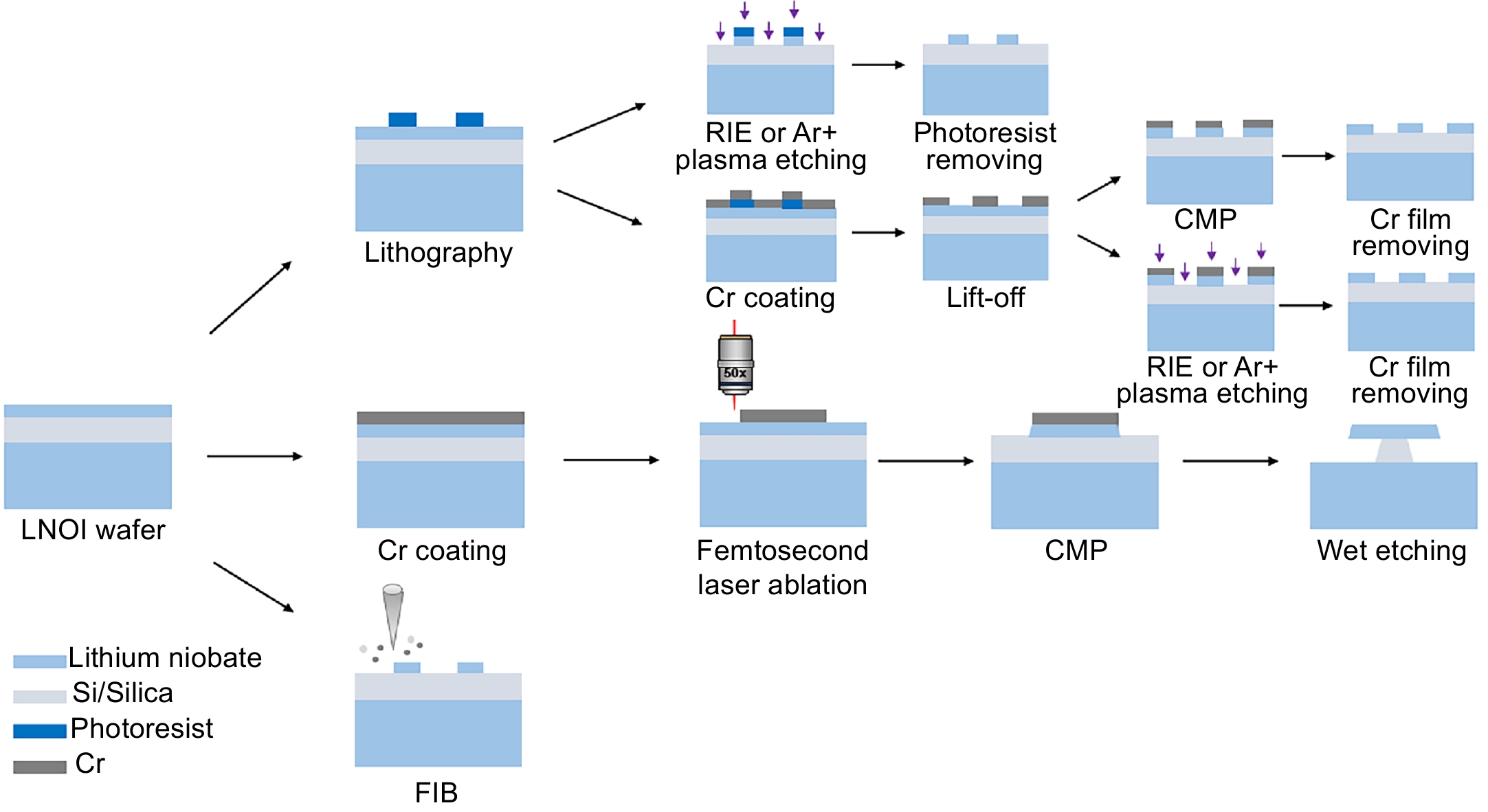
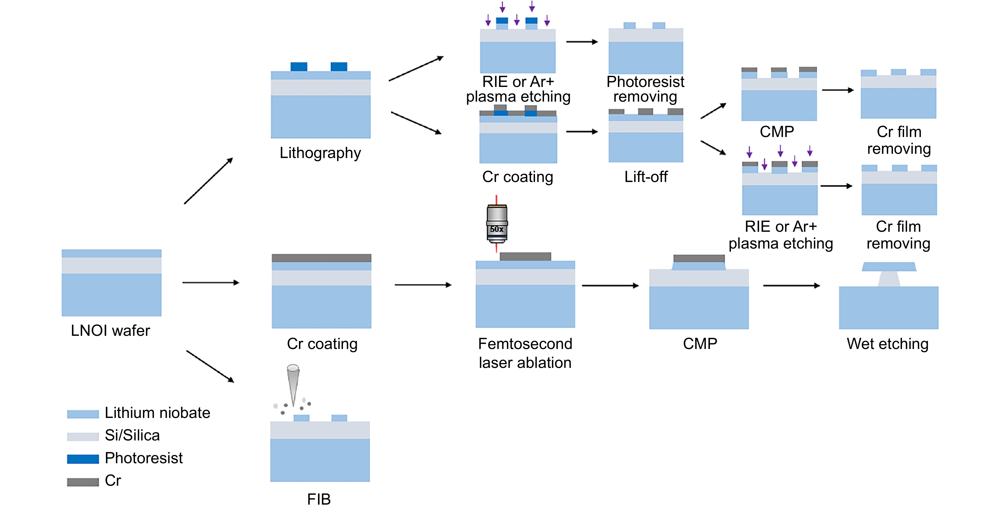
With the rapid development of lithium-niobate-on-insulator (LNOI) thin film technology and related surface micro-nano manufacturing technology in recent years, a series of high-quality and high-performance photonic functional devices on lithium niobate chip have been realized, such as compact modulators with ultra-high performance, broadband frequency combs, as well as high-efficiency optical frequency converters and single-photon sources. Great progress has been made in nonlinear optical frequency conversion, electro-optic modulation and optical passivity. In this paper, we briefly introduce several micro-nano processing technologies that have the potential to produce high-quality lithium niobate metasurfaces, and summarize the recent research progress in optical frequency conversion, electro-optic modulation, optical passivity and other aspects of lithium niobate metasurfaces, and prospected the potential research directions in the field of micro-nano optics.
-

-
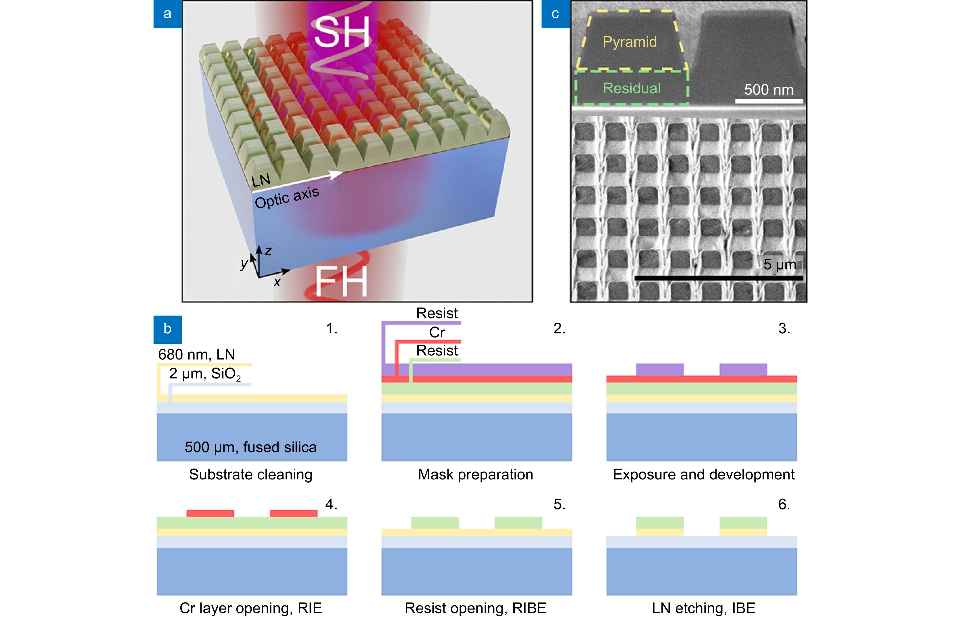
图 2 (a) 铌酸锂超构表面SHG示意图;(b) 制备工艺流程示意图;(c) 所制备超构表面的SEM图像,其中纳米谐振腔由截断金字塔和下面的残余层组成[64]
Figure 2. (a) A schematic of the SHG from the lithium niobate metasurface; (b) Schematic illustration of the process flow of fabrication; (c) SEM image of the fabricated metasurface in which the nanoresonator consists of a truncated pyramid and a residual layer underneath[64]
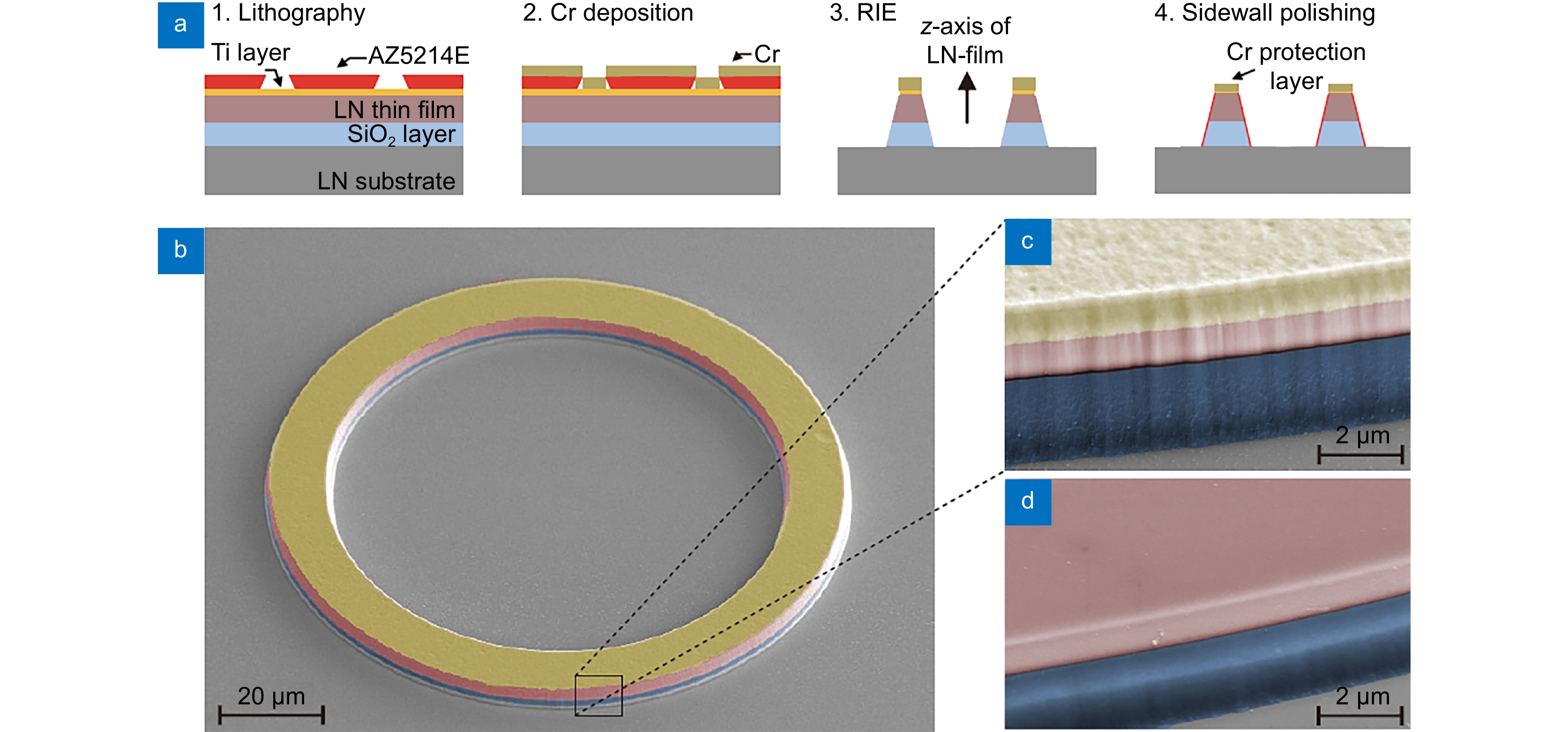
图 4 采用紫外光刻结合RIE技术制备微环腔,然后用CMP抛光侧壁。(a) 制备工艺流程示意图;(b) 微环腔SEM图像;CMP前(c)后(d)微环腔侧壁的放大SEM图像[75]
Figure 4. Microring fabricated by UV lithography and RIE, followed by sidewall polishing by the CMP. (a) Schematic illustration of the process flow of fabrication; (b) False-color SEM image of the microring; and enlarged SEM image of the sidewall (c) before and (d) after the CMP[75]
图 5 (a) 非线性铌酸锂超构表面的SHG示意图。左下插图为D=600 nm的超构表面截面的典型SEM图像,右下插图显示了研究中使用的铌酸锂薄膜的测量二阶极化率;(b) 超构表面SHG效率的光谱依赖性[101]
Figure 5. (a) A schematic of the SHG from the nonlinear lithium niobate metasurface. Left inset gives a typical SEM image of cross section of the metasurface with D=600 nm. Right inset presents the measured second-order susceptibility of the lithium niobate film used in this study; (b) Spectral dependence of SHG efficiencies from metasurfaces[101]
图 6 (a) 铌酸锂超构表面的SPDC:泵浦光从基板侧入射,光子对在反射中收集。泵浦和SPDC光子都沿铌酸锂光轴z偏振;(b) 从量子光学超构表面测量的SPDC光谱。灰色星显示来自未图案化铌酸锂薄膜的SPDC光谱[112]
Figure 6. (a) SPDC from a lithium niobate metasurface: the pump is incident from the substrate side, photon pairs are collected in reflection. Both the pump and the SPDC photons are polarized along the lithium niobate optic axis z; (b) Measured SPDC spectra from quantum optical metasurfaces. Gray stars show the SPDC spectrum from the unpatterned lithium niobate film[112]
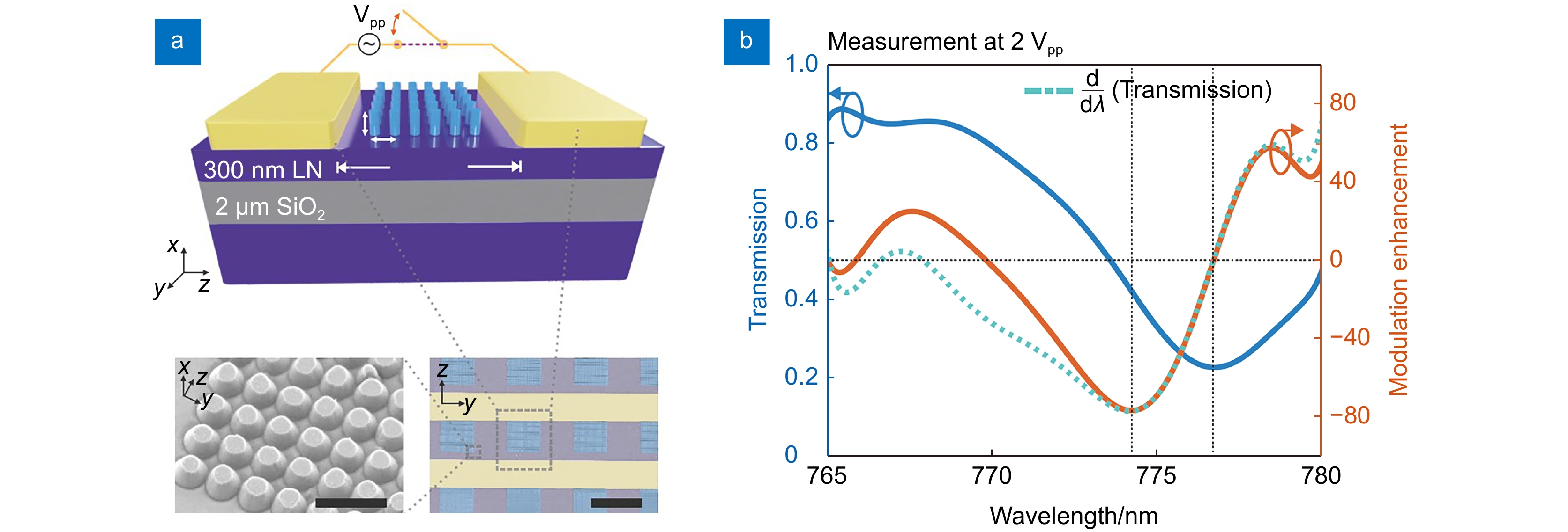
图 7 (a) 由金电极驱动的超构表面结构。左下插图为超构表面柱结构的SEM图像,右下插图显示了电极(黄色)之间几个超构表面(紫色)的伪色SEM;(b) 半径为 135 nm、周期为 500 nm 的超构表面的透射率(蓝色线),橙色线表示 2 VPP和 180 kHz 的交流电压下的调制增强(定义为超构表面的调制幅度除以未图案化区域的调制幅度)[65]
Figure 7. (a) Metasurface driven by Au electrodes. The lower left inset shows the SEM image of the metasurface pillar structure. The lower right inset shows a false-color SEM of several metasurfaces (purple) between the electrodes (yellow); (b) Measured transmission (blue) of a metasurface with radius 135 nm and period 500 nm, normalized by the transmission of an unstructured area. The orange line shows the modulation enhancement, defined as the modulation amplitude of the metasurface divided by the modulation amplitude of an unpatterned area, for an AC voltage of 2 Vpp and 180 kHz[65]
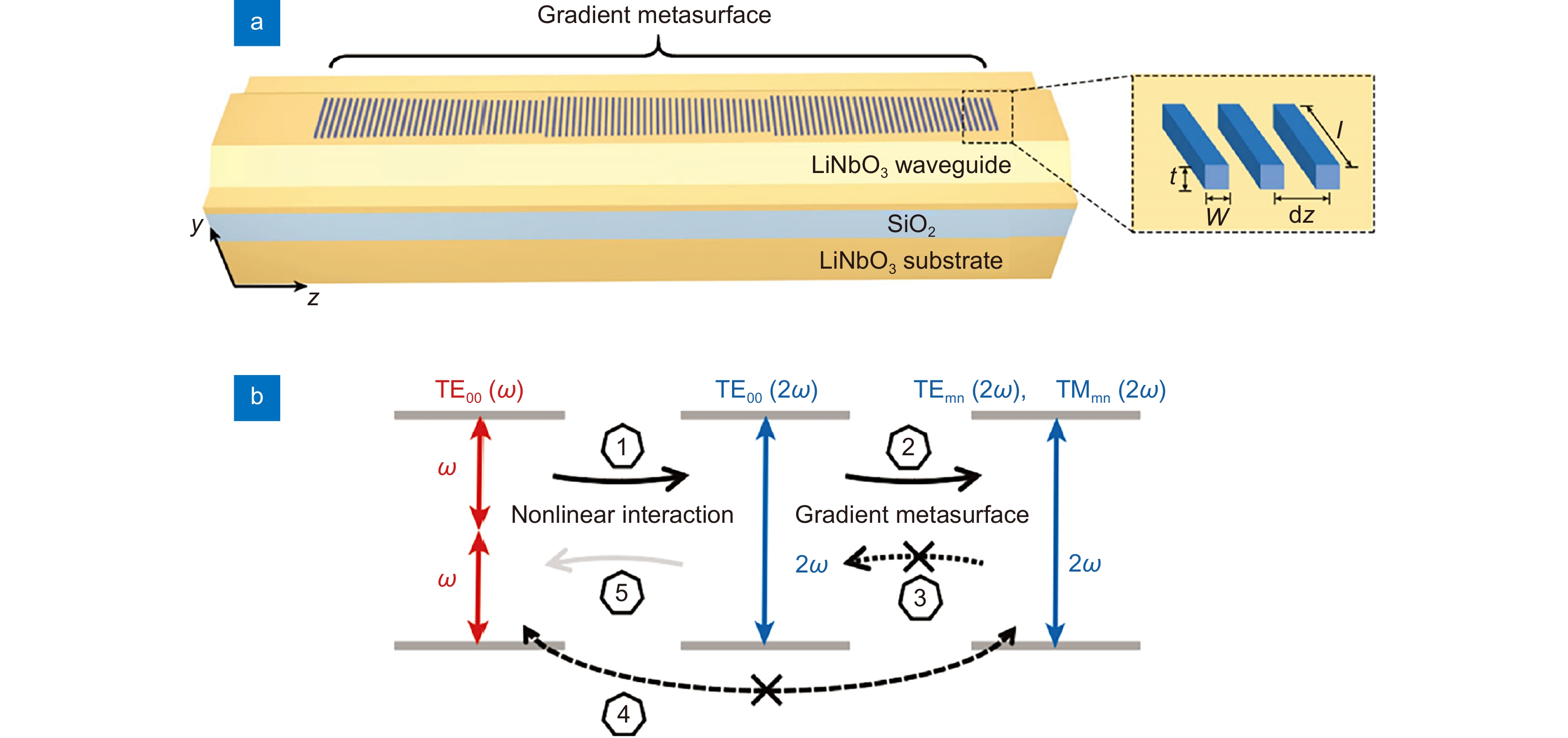
图 8 (a) 集成梯度超构表面的LiNbO3片上脊波导,用于实现无相位匹配的二次谐波产生; (b) 基于超构表面无相位匹配的二次谐波产生原理图[88]
Figure 8. (a) Schematic of the LiNbO3 on-chip ridge waveguide integrated with a well-designed gradient metasurface for achieving phase-matching-free second harmonic generation; (b) Conceptual diagram of the metasurface-based phase-matching-free second harmonic generation[88]
表 1 超构表面SHG主要性能参数
Table 1. Main performance parameters of metasurface SHG
Meta-atoms Size Process technology FH intensity FH wavelength SH wavelength Conversion efficiency Truncated pyramid[59] PT=870 nm
L=700 nmEBL+IBE 4.3 GW/cm2 ~1550 nm ~775 nm ~10−6 Ridge waveguide[86] D=600 nm
d=85 nm
h=235 nmFIB 2.05 GW/cm2 740 nm~1000 nm 370 nm~500 nm 2×10⁻⁶ Cylinder[65] PC=590 nm
R=175 nmFIB 0.5 GW/cm2 825 nm 412 nm 2.9×10⁻⁸ -
参考文献
[1] Zheludev N I, Kivshar Y S. From metamaterials to metadevices[J]. Nat Mater, 2012, 11(11): 917−924. doi: 10.1038/nmat3431
[2] Ren M X, Cai W, Xu J J. Tailorable dynamics in nonlinear optical metasurfaces[J]. Adv Mater, 2020, 32(3): 1806317. doi: 10.1002/adma.201806317
[3] Yu N F, Genevet P, Kats M A, et al. Light propagation with phase discontinuities: generalized laws of reflection and refraction[J]. Science, 2011, 334(6054): 333−337. doi: 10.1126/science.1210713
[4] Li G X, Zhang S, Zentgraf T. Nonlinear photonic metasurfaces[J]. Nat Rev Mater, 2017, 2(1): 17010. doi: 10.1038/natrevmats.2017.10
[5] Krasnok A, Tymchenko M, Alù A. Nonlinear metasurfaces: a paradigm shift in nonlinear optics[J]. Mater Today, 2018, 21(1): 8−21. doi: 10.1016/j.mattod.2017.06.007
[6] Ni X J, Emani N K, Kildishev A V, et al. Broadband light bending with plasmonic nanoantennas[J]. Science, 2012, 335(6067): 427. doi: 10.1126/science.1214686
[7] Boltasseva A, Atwater H A. Low-loss plasmonic metamaterials[J]. Science, 2011, 331(6015): 290−291. doi: 10.1126/science.1198258
[8] Ye W M, Zeuner F, Li X, et al. Spin and wavelength multiplexed nonlinear metasurface holography[J]. Nat Commun, 2016, 7(1): 11930. doi: 10.1038/ncomms11930
[9] Gomes A S L, Maldonado M, de S. Menezes L, et al. Linear and third-order nonlinear optical properties of self-assembled plasmonic gold metasurfaces[J]. Nanophotonics, 2020, 9(4): 725−740. doi: 10.1515/nanoph-2019-0521
[10] Deng J H, Tang Y T, Chen S M, et al. Giant enhancement of second-order nonlinearity of epsilon-near- zero medium by a plasmonic metasurface[J]. Nano Lett, 2020, 20(7): 5421−5427. doi: 10.1021/acs.nanolett.0c01810
[11] Wu W, Ren M X, Pi B, et al. Displacement sensor based on plasmonic slot metamaterials[J]. Appl Phys Lett, 2016, 108(7): 073106. doi: 10.1063/1.4940909
[12] Li Z, Wang C T, Kong W J, et al. Broadband achromatic metasurface filter for apodization imaging in the visible[J]. Opto-Electron Eng, 2021, 48(5): 200466. doi: 10.12086/oee.2021.200466
[13] 张俊卿, 吴毅萍, 陈晟皓, 等. 改进型蝴蝶结超表面及在痕量铅离子检测中的应用[J]. 光电工程, 2021, 48(8): 210123. doi: 10.12086/oee.2021.210123
Zhang J Q, Wu Y P, Chen S H, et al. Optimized bow-tie metasurface and its application in trace detection of lead ion[J]. Opto-Electron Eng, 2021, 48(8): 210123. doi: 10.12086/oee.2021.210123
[14] Li L, Liu Z X, Ren X F, et al. Metalens-array-based high-dimensional and multiphoton quantum source[J]. Science, 2020, 368(6498): 1487−1490. doi: 10.1126/science.aba9779
[15] Liu J, Shi M Q, Chen Z, et al. Quantum photonics based on metasurfaces[J]. Opto-Electron Adv, 2021, 4(9): 200092. doi: 10.29026/oea.2021.200092
[16] Jahani S, Jacob Z. All-dielectric metamaterials[J]. Nat Nanotechnol, 2016, 11(1): 23−36. doi: 10.1038/nnano.2015.304
[17] Kuznetsov A I, Miroshnichenko A E, Brongersma M L, et al. Optically resonant dielectric nanostructures[J]. Science, 2016, 354(6314): aag2472. doi: 10.1126/science.aag2472
[18] Liu H Z, Guo C, Vampa G, et al. Enhanced high-harmonic generation from an all-dielectric metasurface[J]. Nat Phys, 2018, 14(10): 1006−1010. doi: 10.1038/s41567-018-0233-6
[19] Zhu W, Yang R S, Geng G Z, et al. Titanium dioxide metasurface manipulating high-efficiency and broadband photonic spin Hall effect in visible regime[J]. Nanophotonics, 2020, 9(14): 4327−4335. doi: 10.1515/nanoph-2020-0290
[20] Liu S, Vabishchevich P P, Vaskin A, et al. An all-dielectric metasurface as a broadband optical frequency mixer[J]. Nat Commun, 2018, 9(1): 2507. doi: 10.1038/s41467-018-04944-9
[21] Fang C Z, Yang Q Y, Yuan Q C, et al. High-Q resonances governed by the quasi-bound states in the continuum in all-dielectric metasurfaces[J]. Opto-Electron Adv, 2021, 4(6): 200030. doi: 10.29026/oea.2021.200030
[22] Cao T, Lian M, Chen X Y, et al. Multi-cycle reconfigurable THz extraordinary optical transmission using chalcogenide metamaterials[J]. Opto-Electron Sci, 2022, 1(1): 210010. doi: 10.29026/oes.2022.210010
[23] Weis R S, Gaylord T K. Lithium niobate: summary of physical properties and crystal structure[J]. Appl Phys A, 1985, 37(4): 191−203. doi: 10.1007/BF00614817
[24] Kong Y F, Bo F, Wang W W, et al. Recent progress in lithium niobate: optical damage, defect simulation, and on-chip devices[J]. Adv Mater, 2020, 32(3): 1806452. doi: 10.1002/adma.201806452
[25] Arizmendi L. Photonic applications of lithium niobate crystals[J]. Phys Status Solidi (A), 2004, 201(2): 253−283. doi: 10.1002/pssa.200303911
[26] Poberaj G, Hu H, Sohler W, et al. Lithium niobate on insulator (LNOI) for micro-photonic devices[J]. Laser Photon Rev, 2012, 6(4): 488−503. doi: 10.1002/lpor.201100035
[27] Boes A, Corcoran B, Chang L, et al. Status and potential of lithium niobate on insulator (LNOI) for photonic integrated circuits[J]. Laser Photon Rev, 2018, 12(4): 1700256. doi: 10.1002/lpor.201700256
[28] Zhang M, Wang C, Cheng R, et al. Monolithic ultrahigh-Q lithium niobate microring resonator[J]. Optica, 2017, 4(12): 1536−1537. doi: 10.1364/optica.4.001536
[29] Wu R B, Wang M, Xu J, et al. Long Low-loss-litium niobate on insulator waveguides with sub-nanometer surface roughness[J]. Nanomaterials, 2018, 8(11): 910. doi: 10.3390/nano8110910
[30] Wolf R, Breunig I, Zappe H, et al. Scattering-loss reduction of ridge waveguides by sidewall polishing[J]. Opt Express, 2018, 26(16): 19815−19820. doi: 10.1364/OE.26.019815
[31] Siew S Y, Cheung E J H, Liang H D, et al. Ultra-low loss ridge waveguides on lithium niobate via argon ion milling and gas clustered ion beam smoothening[J]. Opt Express, 2018, 26(4): 4421−4430. doi: 10.1364/OE.26.004421
[32] Wang C, Zhang M, Chen X, et al. Integrated lithium niobate electro-optic modulators operating at CMOS-compatible voltages[J]. Nature, 2018, 562(7725): 101−104. doi: 10.1038/s41586-018-0551-y
[33] He M B, Xu M Y, Ren Y X, et al. High-performance hybrid silicon and lithium niobate Mach–Zehnder modulators for 100 Gbit s−1 and beyond[J]. Nat Photonics, 2019, 13(5): 359−364. doi: 10.1038/s41566-019-0378-6
[34] Weigel P O, Zhao J, Fang K, et al. Bonded thin film lithium niobate modulator on a silicon photonics platform exceeding 100 GHz 3-dB electrical modulation bandwidth[J]. Opt Express, 2018, 26(18): 23728−23739. doi: 10.1364/OE.26.023728
[35] Mercante A J, Shi S Y, Yao P, et al. Thin film lithium niobate electro-optic modulator with terahertz operating bandwidth[J]. Opt Express, 2018, 26(11): 14810−14816. doi: 10.1364/OE.26.014810
[36] Zhang M, Buscaino B, Wang C, et al. Broadband electro-optic frequency comb generation in a lithium niobate microring resonator[J]. Nature, 2019, 568(7752): 373−377. doi: 10.1038/s41586-019-1008-7
[37] He Y, Yang Q F, Ling J W, et al. Self-starting bi-chromatic LiNbO3 soliton microcomb[J]. Optica, 2019, 6(9): 1138−1144. doi: 10.1364/OPTICA.6.001138
[38] Wang C, Zhang M, Yu M J, et al. Monolithic lithium niobate photonic circuits for Kerr frequency comb generation and modulation[J]. Nat Commun, 2019, 10(1): 978. doi: 10.1038/s41467-019-08969-6
[39] Wang C, Langrock C, Marandi A, et al. Ultrahigh-efficiency wavelength conversion in nanophotonic periodically poled lithium niobate waveguides[J]. Optica, 2018, 5(11): 1438−1441. doi: 10.1364/OPTICA.5.001438
[40] Chen J Y, Ma Z H, Sua Y M, et al. Ultra-efficient frequency conversion in quasi-phase-matched lithium niobate microrings[J]. Optica, 2019, 6(9): 1244−1245. doi: 10.1364/OPTICA.6.001244
[41] Lu J J, Surya J B, Liu X W, et al. Periodically poled thin-film lithium niobate microring resonators with a second-harmonic generation efficiency of 250, 000%/W[J]. Optica, 2019, 6(12): 1455−1460. doi: 10.1364/OPTICA.6.001455
[42] Elkus B S, Abdelsalam K, Rao A, et al. Generation of broadband correlated photon-pairs in short thin-film lithium-niobate waveguides[J]. Opt Express, 2019, 27(26): 38521−38531. doi: 10.1364/OE.27.038521
[43] Zhao J, Ma C X, Rüsing M, et al. High quality entangled photon pair generation in periodically poled thin-film lithium niobate waveguides[J]. Phys Rev Lett, 2020, 124(16): 163603. doi: 10.1103/PhysRevLett.124.163603
[44] Zhu D, Shao L B, Yu M J, et al. Integrated photonics on thin-film lithium niobate[J]. Adv Opt Photonics, 2021, 13(2): 242−352. doi: 10.1364/AOP.411024
[45] Jia Y C, Wang L, Chen F. Ion-cut lithium niobate on insulator technology: recent advances and perspectives[J]. Appl Phys Rev, 2021, 8(1): 011307. doi: 10.1063/5.0037771
[46] Goodberlet J G, Dunn B L. Deep-ultraviolet contact photolithography[J]. Microelectron Eng, 2000, 53(1–4): 95−99. doi: 10.1016/S0167-9317(00)00272-0
[47] Pease R F W. Electron beam lithography[J]. Contemp Phys, 1981, 22(3): 265−290. doi: 10.1080/00107518108231531
[48] Vieu C, Carcenac F, Pépin A, et al. Electron beam lithography: resolution limits and applications[J]. Appl Surf Sci, 2000, 164(1–4): 111−117. doi: 10.1016/S0169-4332(00)00352-4
[49] Ren Z, Heard P J, Marshall J M, et al. Etching characteristics of LiNbO3 in reactive ion etching and inductively coupled plasma[J]. J Appl Phys, 2008, 103(3): 034109. doi: 10.1063/1.2838180
[50] Deng J, Si G Y, Danner A J. Dry etching of LiNbO3 using inductively coupled plasma[C]//Proceedings of 2010 Photonics Global Conference, 2010: 1–5. doi: 10.1109/PGC.2010.5706006.
[51] Chang C M, Yu C S, Hsieh F C, et al. A parametric study of ICP-RIE etching on a lithium niobate substrate[C]//Proceedings of the 10th IEEE International Conference on Nano/Micro Engineered and Molecular Systems, 2015: 485–486. doi: 10.1109/NEMS.2015.7147473.
[52] Chen G Y, Cheung E J H, Cao Y, et al. Analysis of perovskite oxide etching using argon inductively coupled plasmas for photonics applications[J]. Nanoscale Res Lett, 2021, 16(1): 32. doi: 10.1186/s11671-021-03494-2
[53] Shen C, Wang C L, Zhu Y F, et al. A comparative study of dry-etching nanophotonic devices on a LiNbO3-on-insulator material platform[J]. Proc SPIE, 2021, 11781: 117810X. doi: 10.1117/12.2590415
[54] Wang C, Burek M J, Lin Z N, et al. Integrated high quality factor lithium niobate microdisk resonators[J]. Opt Express, 2014, 22(25): 30924−30933. doi: 10.1364/OE.22.030924
[55] Wang C, Xiong X, Andrade N, et al. Second harmonic generation in nano-structured thin-film lithium niobate waveguides[J]. Opt Express, 2017, 25(6): 6963−6973. doi: 10.1364/OE.25.006963
[56] Hu H, Milenin A P, Wehrspohn R B, et al. Plasma etching of proton-exchanged lithium niobate[J]. J Vac Sci Technol A, 2006, 24(4): 1012−1015. doi: 10.1116/1.2207150
[57] Nagata H, Mitsugi N, Shima K, et al. Growth of crystalline LiF on CF4 plasma etched LiNbO3 substrates[J]. J Cryst Growth, 1998, 187(3–4): 573−576. doi: 10.1016/S0022-0248(98)00009-8
[58] Mitsugi N, Nagata H. Challenges in electron cyclotron resonance plasma etching of LiNbO3 surface for fabrication of ridge optical waveguides[J]. J Vac Sci Technol A, 1998, 16(4): 2245−2251. doi: 10.1116/1.581334
[59] Rusing M, Weigel P O, Zhao J, et al. Toward 3D integrated photonics including lithium niobate thin films: a bridge between electronics, radio frequency, and optical technology[J]. IEEE Nanotechnol Mag, 2019, 13(4): 18−33. doi: 10.1109/MNANO.2019.2916115
[60] Qi Y F, Li Y. Integrated lithium niobate photonics[J]. Nanophotonics, 2020, 9(6): 1287−1320. doi: 10.1515/nanoph-2020-0013
[61] Honardoost A, Abdelsalam K, Fathpour S. Rejuvenating a versatile photonic material: thin-film lithium niobate[J]. Laser Photon Rev, 2020, 14(9): 2000088. doi: 10.1002/lpor.202000088
[62] Wang C, Zhang M, Lončar M. High-Q lithium niobate microcavities and their applications[M]//Xiao Y F, Zou C L, Gong Q H, et al. Ultra-High-Q Optical Microcavities. Singapore: World Scientific, 2020: 1–35. doi: 10.1142/9789814566070_0001.
[63] Sakashita Y, Segawa H. Preparation and characterization of LiNbO3 thin films produced by chemical‐vapor deposition[J]. J Appl Phys, 1995, 77(11): 5995−5999. doi: 10.1063/1.359183
[64] Fedotova A, Younesi M, Sautter J, et al. Second-harmonic generation in resonant nonlinear metasurfaces based on lithium niobate[J]. Nano Lett, 2020, 20(12): 8608−8614. doi: 10.1021/acs.nanolett.0c03290
[65] Weigand H, Vogler-Neuling V V, Escalé M R, et al. Enhanced electro-optic modulation in resonant metasurfaces of lithium niobate[J]. ACS Photonics, 2021, 8(10): 3004−3009. doi: 10.1021/acsphotonics.1c00935
[66] Krasnokutska I, Tambasco J L J, Li X J, et al. Ultra-low loss photonic circuits in lithium niobate on insulator[J]. Opt Express, 2018, 26(2): 897−904. doi: 10.1364/OE.26.000897
[67] Ulliac G, Calero V, Ndao A, et al. Argon plasma inductively coupled plasma reactive ion etching study for smooth sidewall thin film lithium niobate waveguide application[J]. Opt Mater, 2016, 53: 1−5. doi: 10.1016/j.optmat.2015.12.040
[68] Hu H, Ricken R, Sohler W. Etching of lithium niobate: from ridge waveguides to photonic crystal structures[C]//Proceedings of the 14th European Conference on Integrated Optics and Technical Exhibition, 2008: 75–78.
[69] Gui L, Hu H, Garcia-Granda M, et al. Local periodic poling of ridges and ridge waveguides on X- and Y-Cut LiNbO3 and its application for second harmonic generation[J]. Opt Express, 2009, 17(5): 3923−3928. doi: 10.1364/OE.17.003923
[70] Lin J T, Xu Y X, Fang Z W, et al. Fabrication of high-Q lithium niobate microresonators using femtosecond laser micromachining[J]. Sci Rep, 2015, 5: 8072. doi: 10.1038/srep08072
[71] Lin J T, Xu Y X, Fang Z W, et al. Second harmonic generation in a high-Q lithium niobate microresonator fabricated by femtosecond laser micromachining[J]. Sci China Phys Mech Astron, 2015, 58(11): 114209. doi: 10.1007/s11433-015-5728-x
[72] Gao B F, Ren M X, Wu W, et al. Lithium niobate metasurfaces[J]. Laser Photon Rev, 2019, 13(5): 1800312. doi: 10.1002/lpor.201800312
[73] Carletti L, Zilli A, Moia F, et al. Steering and encoding the polarization of the second harmonic in the visible with a monolithic LiNbO3 metasurface[J]. ACS Photonics, 2021, 8(3): 731−737. doi: 10.1021/acsphotonics.1c00026
[74] Wang M, Wu R B, Lin J T, et al. Chemo-mechanical polish lithography: a pathway to low loss large-scale photonic integration on lithium niobate on insulator[J]. Quantum Eng, 2019, 1(1): e9. doi: 10.1002/que2.9
[75] Wolf R, Breunig I, Zappe H, et al. Cascaded second-order optical nonlinearities in on-chip micro rings[J]. Opt Express, 2017, 25(24): 29927−29933. doi: 10.1364/OE.25.029927
[76] Fang Z W, Haque S, Lin J T, et al. Real-time electrical tuning of an optical spring on a monolithically integrated ultrahigh Q lithium nibote microresonator[J]. Opt Lett, 2019, 44(5): 1214−1217. doi: 10.1364/OL.44.001214
[77] Gao R H, Zhang H S, Bo F, et al. Broadband highly efficient nonlinear optical processes in on-chip integrated lithium niobate microdisk resonators of Q-factor above 108[J]. New J Phys, 2021, 23(12): 123027. doi: 10.1088/1367-2630/ac3d52
[78] Gao R H, Yao N, Guan J L, et al. Lithium niobate microring with ultra-high Q factor above 108[J]. Chin Opt Lett, 2022, 20(1): 011902. doi: 10.3788/COL202220.011902
[79] Zhang J H, Fang Z W, Lin J T, et al. Fabrication of crystalline microresonators of high quality factors with a controllable wedge angle on lithium niobate on insulator[J]. Nanomaterials, 2019, 9(9): 1218. doi: 10.3390/nano9091218
[80] Liu S, Sinclair M B, Saravi S, et al. Resonantly enhanced second-harmonic generation using III-V semiconductor all-dielectric metasurfaces[J]. Nano Lett, 2016, 16(9): 5426−5432. doi: 10.1021/acs.nanolett.6b01816
[81] Carletti L, Marino G, Ghirardini L, et al. Nonlinear goniometry by second-harmonic generation in AlGaAs nanoantennas[J]. ACS Photonics, 2018, 5(11): 4386−4392. doi: 10.1021/acsphotonics.8b00810
[82] Carletti L, Rocco D, Locatelli A, et al. Controlling second-harmonic generation at the nanoscale with monolithic AlGaAs-on-AlOx antennas[J]. Nanotechnology, 2017, 28(11): 114005. doi: 10.1088/1361-6528/aa5645
[83] Lin J T, Yao N, Hao Z Z, et al. Broadband quasi-phase-matched harmonic generation in an on-chip monocrystalline lithium niobate microdisk resonator[J]. Phys Rev Lett, 2019, 122(17): 173903. doi: 10.1103/PhysRevLett.122.173903
[84] Lehr D, Reinhold J, Thiele I, et al. Enhancing second harmonic generation in gold nanoring resonators filled with lithium niobate[J]. Nano Lett, 2015, 15(2): 1025−1030. doi: 10.1021/nl5038819
[85] Gigli C, Leo G. All-dielectric χ(2) metasurfaces: recent progress[J]. Opto-Electron Adv, 2022, 5(7): 210093. doi: 10.29026/oea.2022.210093
[86] Wei D Z, Wang C W, Wang H J, et al. Experimental demonstration of a three-dimensional lithium niobate nonlinear photonic crystal[J]. Nat Photonics, 2018, 12(10): 596−600. doi: 10.1038/s41566-018-0240-2
[87] Liang H X, Luo R, He Y, et al. High-quality lithium niobate photonic crystal nanocavities[J]. Optica, 2017, 4(10): 1251−1258. doi: 10.1364/OPTICA.4.001251
[88] Wang C, Li Z Y, Kim M H, et al. Metasurface-assisted phase-matching-free second harmonic generation in lithium niobate waveguides[J]. Nat Commun, 2017, 8(1): 2098. doi: 10.1038/s41467-017-02189-6
[89] Wang L, Wang C, Wang J, et al. High-Q chaotic lithium niobate microdisk cavity[J]. Opt Lett, 2018, 43(12): 2917−2920. doi: 10.1364/OL.43.002917
[90] Boes A, Chang L, Knoerzer M, et al. Improved second harmonic performance in periodically poled LNOI waveguides through engineering of lateral leakage[J]. Opt Express, 2019, 27(17): 23919−23928. doi: 10.1364/OE.27.023919
[91] Rao A, Abdelsalam K, Sjaardema T, et al. Actively-monitored periodic-poling in thin-film lithium niobate photonic waveguides with ultrahigh nonlinear conversion efficiency of 4600%W−1cm−2[J]. Opt Express, 2019, 27(18): 25920−25930. doi: 10.1364/OE.27.025920
[92] Lu J J, Li M, Zou C L, et al. Toward 1% single-photon anharmonicity with periodically poled lithium niobate microring resonators[J]. Optica, 2020, 7(12): 1654−1659. doi: 10.1364/OPTICA.403931
[93] Li M X, Liang H X, Luo R, et al. High-Q 2D lithium niobate photonic crystal slab nanoresonators[J]. Laser Photon Rev, 2019, 13(5): 1800228. doi: 10.1002/lpor.201800228
[94] Minkov M, Gerace D, Fan S H. Doubly resonant χ(2) nonlinear photonic crystal cavity based on a bound state in the continuum[J]. Optica, 2019, 6(8): 1039−1045. doi: 10.1364/OPTICA.6.001039
[95] Shcherbakov M R, Liu S, Zubyuk V V, et al. Ultrafast all-optical tuning of direct-gap semiconductor metasurfaces[J]. Nat Commun, 2017, 8(1): 17. doi: 10.1038/s41467-017-00019-3
[96] Löchner F J F, Fedotova A N, Liu S, et al. Polarization-dependent second harmonic diffraction from resonant GaAs metasurfaces[J]. Acs Photonics, 2018, 5(5): 1786−1793. doi: 10.1021/acsphotonics.7b01533
[97] Kim K H, Rim W S. Anapole resonances facilitated by high-index contrast between substrate and dielectric nanodisk enhance vacuum ultraviolet generation[J]. ACS Photonics, 2018, 5(12): 4769−4775. doi: 10.1021/acsphotonics.8b01287
[98] Huang Z J, Lu H H, Xiong H Q, et al. Fano resonance on nanostructured lithium niobate for highly efficient and tunable second harmonic generation[J]. Nanomaterials, 2019, 9(1): 69. doi: 10.3390/nano9010069
[99] Timpu F, Sendra J, Renaut C, et al. Lithium niobate nanocubes as linear and nonlinear ultraviolet Mie resonators[J]. ACS Photonics, 2019, 6(2): 545−552. doi: 10.1021/acsphotonics.8b01594
[100] Wang J Y, Liu Z J, Xiang J, et al. Ultraviolet second harmonic generation from Mie-resonant lithium niobate nanospheres[J]. Nanophotonics, 2021, 10(17): 4273−4278. doi: 10.1515/nanoph-2021-0326
[101] Ma J J, Xie F, Chen W J, et al. Nonlinear lithium niobate metasurfaces for second harmonic generation[J]. Laser Photon Rev, 2021, 15(5): 2000521. doi: 10.1002/LPOR.202000521
[102] Li Y, Nemilentsau A, Argyropoulos C. Resonance energy transfer and quantum entanglement mediated by epsilon-near-zero and other plasmonic waveguide systems[J]. Nanoscale, 2019, 11(31): 14635−14647. doi: 10.1039/C9NR05083C
[103] Chen Y A, Zhang Q, Chen T Y, et al. An integrated space-to-ground quantum communication network over 4, 600 kilometres[J]. Nature, 2021, 589(7841): 214−219. doi: 10.1038/s41586-020-03093-8
[104] Prevedel R, Walther P, Tiefenbacher F, et al. High-speed linear optics quantum computing using active feed-forward[J]. Nature, 2007, 445(7123): 65−69. doi: 10.1038/nature05346
[105] Daiss S, Langenfeld S, Welte S, et al. A quantum-logic gate between distant quantum-network modules[J]. Science, 2021, 371(6529): 614−617. doi: 10.1126/science.abe3150
[106] Lloyd S. Enhanced sensitivity of photodetection via quantum illumination[J]. Science, 2008, 321(5895): 1463−1465. doi: 10.1126/science.1160627
[107] Barry J F, Turner M J, Schloss J M, et al. Optical magnetic detection of single-neuron action potentials using quantum defects in diamond[J]. Proc Natl Acad Sci USA, 2016, 113(49): 14133−14138. doi: 10.1073/pnas.1601513113
[108] Cheng X, Sarihan M C, Chang K C, et al. Design of spontaneous parametric down-conversion in integrated hybrid SixNy-PPLN waveguides[J]. Opt Express, 2019, 27(21): 30773−30787. doi: 10.1364/OE.27.030773
[109] Introini V, Steel M J, Sipe J E, et al. Spontaneous parametric down conversion in a doubly resonant one-dimensional photonic crystal[J]. Opt Lett, 2020, 45(5): 1244−1247. doi: 10.1364/OL.385741
[110] Nikolaeva A, Frizyuk K, Olekhno N, et al. Directional emission of down-converted photons from a dielectric nanoresonator[J]. Phys Rev A, 2021, 103(4): 043703. doi: 10.1103/PHYSREVA.103.043703
[111] Marino G, Solntsev A S, Xu L, et al. Spontaneous photon-pair generation from a dielectric nanoantenna[J]. Optica, 2019, 6(11): 1416−1422. doi: 10.1364/OPTICA.6.001416
[112] Santiago-Cruz T, Fedotova A, Sultanov V, et al. Photon pairs from resonant metasurfaces[J]. Nano Lett, 2021, 21(10): 4423−4429. doi: 10.1021/acs.nanolett.1c01125
[113] Shaltout A M, Shalaev V M, Brongersma M L. Spatiotemporal light control with active metasurfaces[J]. Science, 2019, 364(6441): eaat3100. doi: 10.1126/science.aat3100
[114] He Q, Sun S L, Zhou L. Tunable/reconfigurable metasurfaces: physics and applications[J]. Research, 2019, 2019: 1849272. doi: 10.34133/2019/1849272
[115] Zeng C, Lu H, Mao D, et al. Graphene-empowered dynamic metasurfaces and metadevices[J]. Opto-Electron Adv, 2022, 5(4): 200098. doi: 10.29026/oea.2022.200098
[116] Nemati A, Wang Q, Ang N S S, et al. Ultra-high extinction-ratio light modulation by electrically tunable metasurface using dual epsilon-near-zero resonances[J]. Opto-Electron Adv, 2021, 4(7): 200088. doi: 10.29026/oea.2021.200088
[117] Nicholls L H, Rodríguez-Fortuño F J, Nasir M E, et al. Ultrafast synthesis and switching of light polarization in nonlinear anisotropic metamaterials[J]. Nat Photonics, 2017, 11(10): 628−633. doi: 10.1038/s41566-017-0002-6
[118] Yin X H, Schäferling M, Michel A K U, et al. Active chiral plasmonics[J]. Nano Lett, 2015, 15(7): 4255−4260. doi: 10.1021/nl5042325
[119] Duan X Y, Kamin S, Liu N. Dynamic plasmonic colour display[J]. Nat Commun, 2017, 8: 14606. doi: 10.1038/ncomms14606
[120] Karvounis A, Vogler-Neuling V V, Richter F U, et al. Electro-optic metasurfaces based on barium titanate nanoparticle films[J]. Adv Opt Mater, 2020, 8(17): 2000623. doi: 10.1002/adom.202000623
[121] Wooten E L, Kissa K M, Yi-Yan A, et al. A review of lithium niobate modulators for fiber-optic communications systems[J]. IEEE J Sel Top Quantum Electron, 2000, 6(1): 69−82. doi: 10.1109/2944.826874
[122] Li M X, Ling J W, He Y, et al. Lithium niobate photonic-crystal electro-optic modulator[J]. Nat Commun, 2020, 11(1): 4123. doi: 10.1038/s41467-020-17950-7
[123] Bo F, Wang J, Cui J, et al. Lithium-niobate–silica hybrid whispering-gallery-mode resonators[J]. Adv Mater, 2015, 27(48): 8075−8081. doi: 10.1002/adma.201504722
[124] Timpu F, Weigand H, Kaufmann F, et al. Towards active electro-optic lithium niobate metasurfaces[J]. EPJ Web Conf, 2020, 238: 05003. doi: 10.1051/epjconf/202023805003
[125] Gao B F, Ren M X, Wu W, et al. Electro-optic lithium niobate metasurfaces[J]. Sci China Phys Mech Astron, 2021, 64(4): 240362. doi: 10.1007/s11433-021-1668-y
[126] Maker P D, Terhune R W, Nisenoff M, et al. Effects of dispersion and focusing on the production of optical harmonics[J]. Phys Rev Lett, 1962, 8(1): 21−22. doi: 10.1103/PhysRevLett.8.21
[127] Armstrong J A, Bloembergen N, Ducuing J, et al. Interactions between light waves in a nonlinear dielectric[J]. Phys Rev, 1962, 127(6): 1918−1939. doi: 10.1103/PhysRev.127.1918
[128] Chen J Y, Sua Y M, Fan H, et al. Modal phase matched lithium niobate nanocircuits for integrated nonlinear photonics[J]. OSA Continuum, 2018, 1(1): 229−242. doi: 10.1364/OSAC.1.000229
[129] Fang B, Li H M, Zhu S N, et al. Second-harmonic generation and manipulation in lithium niobate slab waveguides by grating metasurfaces[J]. Photonics Res, 2020, 8(8): 1296−1300. doi: 10.1364/PRJ.391850
[130] Fang B, Wang Z Z, Gao S L, et al. Manipulating guided wave radiation with integrated geometric metasurface[J]. Nanophotonics, 2022, 11(9): 1923−1930. doi: 10.1515/nanoph-2021-0466
[131] Zhang D, Ren M X, Wu W, et al. Nanoscale beam splitters based on gradient metasurfaces[J]. Opt Lett, 2018, 43(2): 267−270. doi: 10.1364/OL.43.000267
[132] Wang R D, Wu Q, Zhang Y Q, et al. Enhanced on-chip terahertz sensing with hybrid metasurface/lithium niobate structures[J]. Appl Phys Lett, 2019, 114(12): 121102. doi: 10.1063/1.5087609
-
访问统计


 E-mail Alert
 RSS
RSS
 下载:
下载:
