Optical characteristics of one dimensional metal-dielectric photonic band gap material
-
摘要:
本文描述了由不同厚度的ITO和Ag层制成的一维金属介质光子带隙材料1D M-D PBG的光学透射和反射特性。研究发现,单元尺寸小于80 nm的金属结构和较小的金属分数会导致光学透射率的提高。对于大于80 nm的单元尺寸,在可见光的低频和高频的频谱范围内反射率都相应增强。这是由于一种特殊结构和等离子体的带隙的作用。此外,在两个范围内的反射随着增加银膜厚度的增加而提高和扩大。结构引起的反射光谱随着单位尺寸的增大而增大,并且由于等离子体光子带隙的反射超出光学范围。研究结果对1D M-D PBG光学滤波器的设计有一定的参考价值。
Abstract:This paper describes the optical transmittance and reflection of one dimensional metal-dielectric photonic-band gap material (1D M-D PBG), which is made of different thicknesses ITO and Ag layers. It is found that structures with a unit size below 80 nm and a smaller metal fraction leads to improvement of optical transmittance. For unit sizes larger than 80 nm, the reflection at the shorter and longer wavelengths increases. This is due to the generation of a structural and plasmonic band gap. In addition, the reflection in both ranges increases and broadens by increasing Ag films thicknesses. The reflection spectrum induced by structure shifts towards longer wavelength as a result of unit size increasing and the reflection due to plasmonic band gap piles beyond to optical range. The results are very useful for optical filter of 1D M-D PBG design.

-
Key words:
- metal photo crystals /
- optical transmittance /
- optical reflection
-

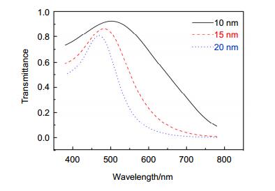
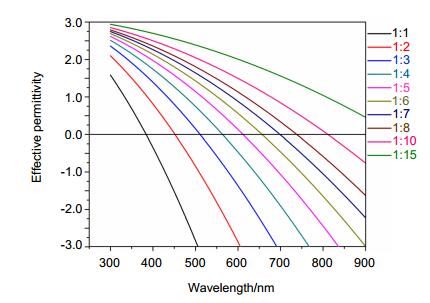
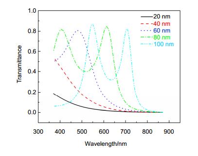
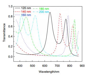
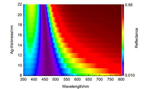
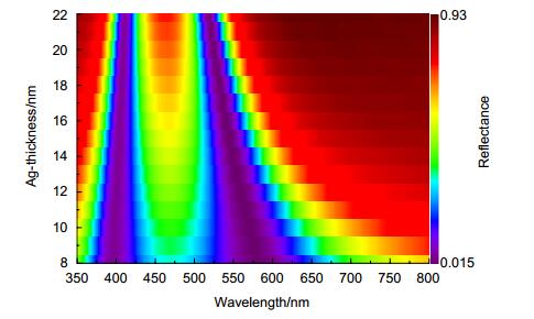
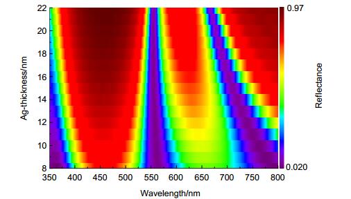
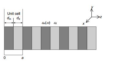
Overview: This paper describes the optical transmittance and reflection of one dimensional metal-dielectric photonic-band gap material (1D M-D PBG), which is made of different thicknesses ITO and Ag layers. In this paper, there are two crucial factors determining optical transmittance were taken into account. One factor is that a structure band gap presents in the optical structure when the unit size is larger than 80 nm. The other factor is that the plasmonic band gap extends into the optical region with high metal fraction. The two factors have been never been discussed in past. The results are very helpful for visual color design and optical filter production using 1D M-D PBGs. The paper suggested that 1D M-D PBGs with lower than 100 nm ITO films favor to enhance their optical transmittance, and the structures with longer ITO films can induce improvement of optical reflection. In addition, both the reflection in structure and plasmonic band gap increases and broadens by increasing Ag films fraction. The reflection spectrum induced by structure and plasmonic shifts towards longer wavelength as a result of unit size and metal fraction increasing. It is found that the incorporation of thicker dielectric layers can enhance optical transparency when the ITO film thickness is lower than 80 nm. Once the thickness of ITO films included in 1D M-D PBG is below 60 nm, a peak appears in the transmission spectrum, and a minimum reflective band appears in the reflection spectrum. When each ITO layer is thicker than 60 nm, two transmission peaks and two reflective minima appear in the transmission and reflection spectra. In addition, the distance between the two reflective minima decreases as the ITO thickness increasing. Both the structure and plasmonic band gaps are broadened and deeper as the each thickness of Ag films becoming thicker. Once the each thickness of ITO films is 120 nm, there is a deeper structure band gap near the 450 nm. The reflection also enhance by improving the thickness of Ag films. As a result, both optical transmission and reflection can be adjusted by adopting appropriate structure. The results are very helpful for visual color design and optical filter production using 1D M-D PBGs.
-

-
Table 1. Characteristics of 1D-PBG with 3.5 pairs of Ag/ITO layers consisting of 120 nm, 140 nm, 160 nm, 180 nm, and 200 nm ITO films, respectively, and a fixed Ag films thickness of 20 nm
Sample structure
(dd, dm, a, n)Band gap range
(λ1~λ2)/nmBand gap
(λ2-λ1)/nmCentral wavelength Δλ/nm (140, 20, 160, 3.5) 427~628 201 527 - (160, 20, 180, 3.5) 496~755 259 625 98 (180, 20, 200, 3.5) 551~815 264 683 58 (200, 20, 220, 3.5) 597~863 266 726 43 -
[1] Jena S, Tokas R B, Sarkar P, et al. Omnidirectional photonic band gap in magnetron sputtered TiO2/SiO2 one dimensional photonic crystal[J]. Thin Solid Films, 2016, 599: 138-144. doi: 10.1016/j.tsf.2015.12.069
[2] Shen H Z, Wang Z H, Wu Y X, et al. One-dimensional photonic crystals: fabrication, responsiveness and emerging applications in 3D construction[J]. RSC Advances, 2016, 6(6): 4505-4520. doi: 10.1039/C5RA21373H
[3] Moslemi F, Jamshidi-Ghaleh K. Electrically tunable optical bistability based on one-dimensional photonic crystals with nonlinear nanocomposite materials[J]. Journal of Applied Physics, 2016, 119(9): 093101. doi: 10.1063/1.4942866
[4] Xiao X, Wang W J, Li S H, et al. Investigation of defect modes with Al2O3 and TiO2 in one-dimensional photonic crystals[J]. Optik-International Journal for Light and Electron Optics, 2016, 127(1): 135-138. doi: 10.1016/j.ijleo.2015.10.005
[5] Degli-Eredi I, Sipe J E, Vermeulen N. TE-polarized graphene modes sustained by photonic crystal structures[J]. Optics Letters, 2015, 40(9): 2076-2079. doi: 10.1364/OL.40.002076
[6] Luo Z M, Chen M, Deng J Y, et al. Low-pass spatial filters with small angle-domain bandwidth based on one-dimensional metamaterial photonic crystals[J]. Optik-International Journal for Light and Electron Optics, 2016, 127(1): 259-262. doi: 10.1016/j.ijleo.2015.10.034
[7] Liu Y Q, Qi X Y, Lu Y, et al. Observation of beam deflection in one-dimensional photonic lattice in LiNbO3 crystal accompanied with self-focusing and self-defocusing nonlinearities[J]. Physics Letters A, 2016, 380(1-2): 322-325. doi: 10.1016/j.physleta.2015.10.025
[8] Xiao X Y, Chen R P. Study of omnidirectional reflection bandgap extension in one-dimensional quasi-periodic metallic photonic crystal[J]. Nano, 2015, 10(6): 1550088. doi: 10.1142/S1793292015500885
[9] Pavlichenko I, Broda E, Fukuda Y, et al. Bringing one-dimensional photonic crystals to a new light: an electrophotonic platform for chemical mass transport visualisation and cell monitoring[J]. Materials Horizons, 2015, 2(3): 299-308. doi: 10.1039/C4MH00195H
[10] Yu W J, Jia X, Long Y B, et al. Highly efficient semitransparent polymer solar cells with color rendering index approaching 100 using one-dimensional photonic crystal[J]. ACS Applied Materials & Interfaces, 2015, 7(18): 9920-9928.
[11] Mandal S, Bose C, Bose M K. A generalized design of one dimensional photonic crystal based optical filter with lossy materials[J]. Optical and Quantum Electronics, 2016, 48(3): 200. doi: 10.1007/s11082-016-0460-y
[12] Zhao Y L, Ma F H, Li X F, et al. A transparent electromagnetic-shielding film based on one-dimensional metal-dielectric periodic structures[J]. Chinese Physics B, 2018, 27(2): 027302. doi: 10.1088/1674-1056/27/2/027302
[13] Zhao Y L, Li X F, Ma J J, et al. Low-resistant and high transmittance films based on one dimensional metal-dielectric photonic band gap material[J]. Superlattices and Microstructures, 2017, 112: 596-603. doi: 10.1016/j.spmi.2017.10.015
[14] Zhao Y L, Ma F H, Li X F, et al. A transparent electromagnetic-shielding film based on one-dimensional metal-dielectric periodic structures[J]. Chinese Physics B, 2018, 27(2):027302. doi: 10.1088/1674-1056/27/2/027302
[15] Aly A H, Ryu S W, Hsu H T, et al. THz transmittance in one-dimensional superconducting nanomaterial-dielectric superlattice[J]. Materials Chemistry and Physics, 2009, 113(1): 382-384. doi: 10.1016/j.matchemphys.2008.07.123
[16] 赵亚丽, 贾琨, 张晗, 等.金属光子晶体薄膜可见光和微波波段传输性能[J].光电工程, 2017, 44(2): 226-233. doi: 10.3969/j.issn.1003-501X.2017.02.013
Zhao Y L, Jia K, Zhang H, et al. Transmission properties of metal photonic crystal films in visible light and microwave[J]. Opto-Electronic Engineering, 2017, 44(2): 226-233. doi: 10.3969/j.issn.1003-501X.2017.02.013
[17] Scalora M, Bloemer M J, Pethel A S, et al. Transparent, metallo-dielectric, one-dimensional, photonic band-gap structures[J]. Journal of Applied Physics, 1988, 83(5): 2377-2383. http://ieeexplore.ieee.org/xpl/freeabs_all.jsp?arnumber=5020698
[18] Bloemer M J, Scalora M. Transmissive properties of Ag/MgF2 photonic band gaps[J]. Applied Physics Letters, 1988, 72(14): 1676-1678. http://scitation.aip.org/content/aip/journal/apl/72/14/10.1063/1.121150
[19] Ward A J, Pendry J B, Stewart W J. Photonic dispersion surfaces[J]. Journal of Physics: Condensed Matter, 1995, 7(10): 2217-2224. doi: 10.1088/0953-8984/7/10/027
[20] Pradhan S K, Xiao B, Skuza J R, et al. Effects of dielectric thickness on optical behavior and tunability of one-dimensional Ag/SiO2 multilayered metamaterials[J]. Optics Express, 2014, 22(10): 12486-12498. doi: 10.1364/OE.22.012486
[21] Aly A H, Ismaeel M, Abdel-Rahman E. Comparative study of the one dimensional dielectric and metallic photonic crystals[J]. Optics and Photonics Journal, 2012, 2(2): 105-112. doi: 10.4236/opj.2012.22014
[22] Oskooi A F, Roundy D, Ibanescu M, et al. MEEP: a flexible free-software package for electromagnetic simulations by the FDTD method[J]. Computer Physics Communications, 2010, 181(3): 687-702. doi: 10.1016/j.cpc.2009.11.008
[23] 赵亚丽, 马富花, 江波, 等. ITO/Ag光子晶体薄膜的制备及性能[J].光学 精密工程, 2015, 23(6): 1512-1516. http://www.wanfangdata.com.cn/details/detail.do?_type=perio&id=gxjmgc201506003
Zhao Y L, Ma F H, Jiang B, et al. Preparation and properties of ITO/Ag photonic crystal thin films[J]. Optics and Precision Engineering, 2015, 23(6): 1512-1516. http://www.wanfangdata.com.cn/details/detail.do?_type=perio&id=gxjmgc201506003
[24] Cai W S, Shalaev V. Optical Metamaterials: Fundamentals and Applications[M]. New York: Springer, 2010.
[25] Guo Y H, Yan L S, Pan W, et al. A plasmonic splitter based on slot cavity[J]. Optics Express, 2011, 19(15): 13831-13838. doi: 10.1364/OE.19.013831
[26] Guo Y H, Yan L S, Pan W, et al. Electromagnetically induced transparency(EIT)-like transmission in side-coupled complementary split-ring resonators[J]. Optics Express, 2012, 20(22): 24348-24355. doi: 10.1364/OE.20.024348
[27] Wood B, Pendry J B, Tsai D P. Directed subwavelength imaging using a layered metal-dielectric system[J]. Physical Review B, 2006, 74(11): 115116. doi: 10.1103/PhysRevB.74.115116
[28] Belov P A, Hao Y, Subwavelength imaging at optical frequencies using a transmission device formed by a periodic layered metal-dielectric structure operating in the canalization regime[J]. Physical Review B, 2006, 73(11): 113110. doi: 10.1103/PhysRevB.73.113110
-


 E-mail Alert
 RSS
RSS
 下载:
下载:
