
 E-mail Alert
 RSS
RSS
-
摘要
超表面是一种可实现多功能超常电磁调控的超薄型二维阵列平面。它由超材料结构单元组成,可以灵活有效地操控电磁波的相位、极化方式、传播模式等特性,因而在可控智能表面、新型波导结构、电磁波吸收和小型谐振器件等方面展现了广阔的应用前景。本文介绍了超表面的基本概念和背景,同时总结论述了红外和太赫兹波段下,实现完美吸收表面、宽带吸收以及可调吸收等几种超表面器件的设计与发展思路,最后对其潜在问题以及未来趋势进行讨论。
Abstract
The metasurface is an ultra-thin two-dimensional planar array that enables multi-functional and extraordinary electro-magnetic control. It consists of structural units of metamaterials which can flexibly and effectively control the phase, polarization mode and propagation mode of electromagnetic waves. Therefore, it shows great potentials and prospects in various applications including the controllable "smart" surfaces, novel waveguide structures, electromagnetic wave absorption and the miniaturized cavity resonators. In this review, we first introduce basic concepts and background of metasurfaces, and then summarize the design and development of several absorptive metasurface devices in the infrared & terahertz (THz) bands and finally discuss its potential problems and prospective in future.
-
Key words:
- metasurface /
- perfect absorption /
- broadband absorption /
- tunable metasurface
-
Overview

Overview: Infrared photodetectors have been widely used in the fields of military and national economy including aeronautics and astronautics, optical communication, industrial control and so on. The high infrared absorption rate is extremely important for the signal response of the photodetectors. However, the sensitive element of the infrared photodetector does not have good infrared absorption characteristics, so it needs a material that can improve the infrared absorption rate. Among them, metamaterials are widely concerned by researchers because of their novel and non-traditional properties. Metamaterials are typically engineered by arranging a set of small scatterers in a regular array throughout a region of space, thus obtaining some desirable bulk electromagnetic behaviors. The desired property is often the one that is not normally found in nature (negative refractive index, near-zero index, and so on). With the deepening of research, researchers began to expand in the application of metamaterials, and proposed different models, such as metasurfaces, metadevices.
For many applications, metasurfaces can be used take place of metamaterials. Compared to three-dimensional metamaterial structures, metasurfaces have the advantage of taking up less physical space. Consequently, metasurfaces offer the possibility of realizing less-lossy structures.
In this review, we describe the research progress of several common absorption metasurfaces in recent years. The first one is the perfect metasurfaces absorber, which has the ability to absorb all incident waves at a single frequency. By optimizing the structural model, the perfect metasurface absorbers achieve impedance matching with free space, and use the dielectric loss and ohmic loss of the structural unit to achieve strong absorption of electromagnetic waves. However, as the result of relying on resonance absorption, the absorption spectrum of perfect metasurface absorbers is very narrow. Then, the metasurfaces of broadband absorption in the infrared, terahertz and visible light bands are reviewed in detail. And the most common way to achieve broadband absorption of metasurfaces is to use a vertically cascaded structure. In addition, metasurfaces can also achieve broadband absorption by combining graphene or catenary optics. Finally, tunability of the PCM metasurface absorber has also been investigated.
-

-
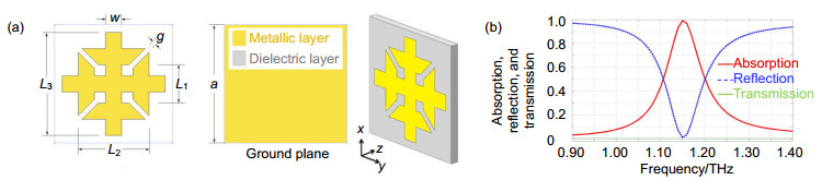
图 2 (a) 单个谐振器结构图;(b)垂直入射时单个谐振器结构的吸收光谱;(c)吸收器基本结构图;(d)吸收器的吸收谱图;(e)双层宽带超表面结构图;(f)双层吸收谱图[20]
Figure 2. (a) Schematic of the single resonator; (b) Simulated absorption spectra of the single resonator at the normal incidence; (c) Schematic of the single-layered GMBA (gradient-metasurface-based absorber); (d) Simulated absorption spectra of the single-layered GMBA; (e) Schematic of the dual-layered GMBA; (f) Simulated absorption spectra of the dual-layered GMBA for TE (black) and TM (red) polarizations
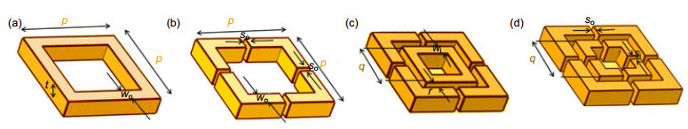


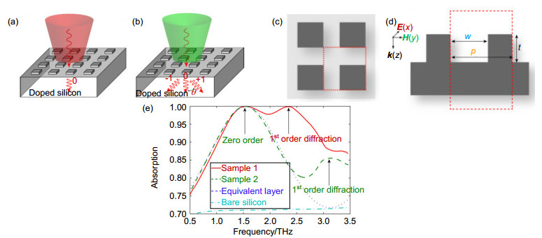
图 6 两种不同频率下的衍射示意图。(a)在衬底中只发生低频零阶衍射;(b)高频率下同时发生零阶衍射和一阶衍射;(c),(d)为该吸波器单元结构的正面及侧面图;(e)不同周期样品、裸掺杂硅片以及四分之一波长抗反射层的吸收谱图[38]
Figure 6. Schematic of diffraction when illuminated at two different frequencies. (a) Only zeroorder diffraction occurs in the substrate at low frequency; (b) First order diffraction in the substrate occurs at higher frequency; (c) and (d) are the front and side views of the structure; (e) Absorption spectra of samples with different periods. The cases for a bare doped silicon slab and an absorber based on quarter-wavelength antireflection layer are also shown[38]
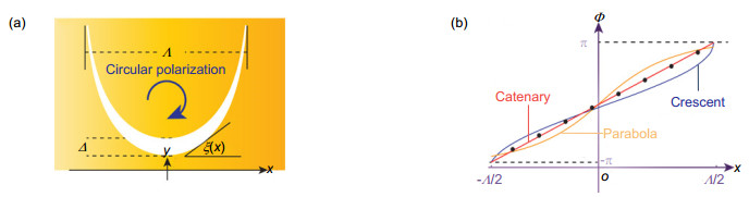
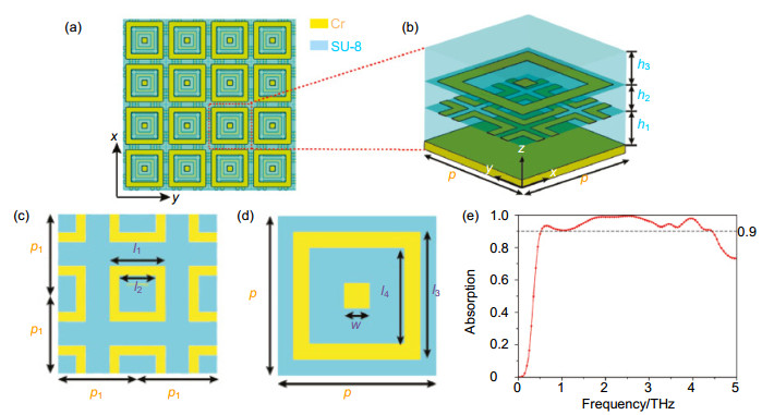
图 8 宽带THz吸收器原理图及仿真结果。(a)俯视图;(b)三维示意图;(c), (d)超表面1和超表面2的几何视图参数;(e)正常入射下的模拟吸收谱[42]
Figure 8. Schematic structure of the broadband THz absorber and the simulated results. (a) Top view of the arrays; (b) Three-dimensional schematic diagram; Top views of (c) metasurface 1 and (d) metasurface 2 with geometric parameters; (e) Simulated absorption spectra at normal incidence in the frequency range from 0 to 5 THz. The analytical catenary field model of dual-metasurface[42]
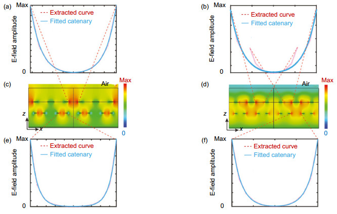
图 9 提取超表面谐振腔和相邻谐振腔两臂之间的电场振幅(红色虚线),拟合悬链线曲线(蓝色实线),分别为0.6 THz((a),(e))和2.5 THz ((b),(f));(c),(d)在两个共振频率下的x-z平面中的电场分布[42]
Figure 9. Extracted electric field amplitude (red dotted line) and fitting catenary curve (blue solid line) between two arms of the resonator and adjacent resonators for the dual metasurface at 0.6 THz (a), (e) and 2.5 THz (b), (f); (c), (d) Electric field distribution in the x-z plane at two resonant frequencies[42]
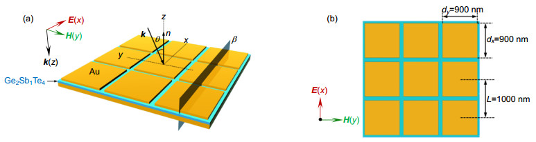
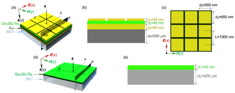
图 12 (a) 超表面结构示意图;(b)超表面结构侧视图;(c)超表面结构俯视图;(d)单层Ge2Sb2Te5介质层结构示意图;(e)单层Ge2Sb2Te5介质层结构侧视图[46]
Figure 12. (a) Schematic of the metamaterial absorber and the incident light polarization configuration; (b) Side view of the absorber; (c) Top view of the absorber; (d) Schematic of the single Ge2Sb2Te5 dielectric layer of 1000 nm × 1000 nm × 40 nm deposited on a BK7 silica glass and the incident light polarization configuration[46]
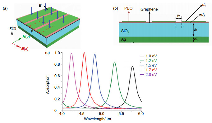
图 14 基于石墨烯的超表面吸收器的原理图。(a)透视图;(b)横截面图;(c)不同化学势下的GMA的吸收光谱[52]
Figure 14. The schematic diagram of the graphene-based metamaterial absorber. (a) The perspective view; (b) The cross sectional view of the GMA(graphene-based metamaterial absorber); (c) The effect of different chemical potential of GMA on the absorption spectra[52]
-
参考文献
[1] 张健, 张文彦, 奚正平.隐身吸波材料的研究进展[J].稀有金属材料与工程, 2008, 37(S4): 504-508. http://d.old.wanfangdata.com.cn/Periodical/xdtlytz200506004
Zhang J, Zhang W Y, Xi Z P. Development of stealth radarwave absorbing materials[J]. Rare Metal Materials and Engineering, 2008, 37(S4): 504-508. http://d.old.wanfangdata.com.cn/Periodical/xdtlytz200506004
[2] 杨长胜, 程海峰, 李效东, 等.智能隐身材料的研究现状[J].功能材料, 2005, 36(5): 643-647. doi: 10.3321/j.issn:1001-9731.2005.05.001
Yang C S, Cheng H F, Li X D, et al. Present status of intelligent stealth material[J]. Journal of Functional Materials, 2005, 36(5): 643-647. doi: 10.3321/j.issn:1001-9731.2005.05.001
[3] Nemati A, Wang Q, Hong M H, et al. Tunable and reconfigurable metasurfaces and metadevices[J]. Opto-Electronic Advances, 2018, 1(5): 180009. doi: 10.29026/oea.2018.180009
[4] Pendry J B, Holden A J, Robbins D J, et al. Magnetism from conductors and enhanced nonlinear phenomena[J]. IEEE Transactions on Microwave Theory and Techniques, 1999, 47(11): 2075-2084. doi: 10.1109/22.798002
[5] Schurig D, Mock J J, Justice B J, et al. Metamaterial electro- magnetic cloak at microwave frequencies[J]. Science, 2006, 314(5801): 977-980. doi: 10.1126/science.1133628
[6] Karvounis A, Gholipour B, MacDonald K F, et al. All-dielectric phase-change reconfigurable metasurface[J]. Applied Physics Letters, 2016, 109(5): 051103. doi: 10.1063/1.4959272
[7] Aieta F, Genevet P, Kats M A, et al. Aberration-free ultrathin flat lenses and axicons at telecom wavelengths based on plasmonic metasurfaces[J]. Nano Letters, 2012, 12(9): 4932-4936. doi: 10.1021/nl302516v
[8] West P R, Stewart J L, Kildishev A V, et al. All-dielectric subwavelength metasurface focusing lens[J]. Optics Express, 2014, 22(21): 26212-26221. doi: 10.1364/OE.22.026212
[9] Holloway C L, Kuester E F, Gordon J A, et al. An overview of the theory and applications of metasurfaces: the two-dimensional equivalents of metamaterials[J]. IEEE Antennas and Propagation Magazine, 2012, 54(2): 10-35. doi: 10.1109/map.2012.6230714
[10] Caniou J. Passive Infrared Detection: Theory and Applications[M]. New York: Springer, 1999: 225.
[11] Jiang X D, Itzler M A, Ben-Michael R, et al. InGaAsP-InP avalanche photodiodes for single photon detection[J]. IEEE Journal of Selected Topics in Quantum Electronics, 2007, 13(4): 895-905. doi: 10.1109/JSTQE.2007.903001
[12] Wang J L, Fang H H, Wang X D, et al. Recent progress on localized field enhanced two‐dimensional material photodetectors from ultraviolet-visible to infrared[J]. Small, 2017, 13(35): 1700894. doi: 10.1002/smll.201700894
[13] 吴国安, 罗林保.近红外光电探测器的发展与应用[J].物理, 2018, 47(3): 137-142. http://d.old.wanfangdata.com.cn/Periodical/wl201803001
Wu G A, Luo L B. Development and application of near infrared photodetectors[J]. Physics, 2018, 47(3): 137-142. http://d.old.wanfangdata.com.cn/Periodical/wl201803001
[14] 于宏岩, 张强, 付淑芳, 等.超表面吸收特性的研究进展[J].哈尔滨师范大学自然科学学报, 2017, 33(6): 33-38. doi: 10.3969/j.issn.1000-5617.2017.06.008
Yu H Y, Zhang Q, Fu S F, et al. Research advances of absorption properties of metasurfaces[J]. Natural Science Journal of Harbin Normal University, 2017, 33(6): 33-38. doi: 10.3969/j.issn.1000-5617.2017.06.008
[15] Yoon G, So S, Kim M, et al. Electrically tunable metasurface perfect absorber for infrared frequencies[J]. Nano Convergence, 2017, 4(1): 36. doi: 10.1186/s40580-017-0131-0
[16] Chen H T, Taylor A J, Yu N F. A review of metasurfaces: physics and applications[J]. Reports on Progress in Physics, 2016, 79(7): 076401. doi: 10.1088/0034-4885/79/7/076401
[17] Chen K, Adato R, Altug H. Dual-band perfect absorber for multispectral plasmon-enhanced infrared spectroscopy[J]. ACS Nano, 2012, 6(9): 7998-8006. doi: 10.1021/nn3026468
[18] Astorino M D, Frezza F, Tedeschi N. Ultra-thin narrow-band, complementary narrow-band, and dual-band metamaterial absorbers for applications in the THz regime[J]. Journal of Applied Physics, 2017, 121(6): 063103. doi: 10.1063/1.4975687
[19] Feng Q, Pu M B, Hu C G, et al. Engineering the dispersion of metamaterial surface for broadband infrared absorption[J]. Optics Letters, 2012, 37(11): 2133-2135. doi: 10.1364/OL.37.002133
[20] Guo W L, Liu Y X, Han T C. Ultra-broadband infrared metasurface absorber[J]. Optics Express, 2016, 24(18): 20586-20592. doi: 10.1364/OE.24.020586
[21] Garnett E, Yang P D. Light trapping in silicon nanowire solar cells[J]. Nano Letters, 2010, 10(3): 1082-1087. doi: 10.1021/nl100161z
[22] Jeong S, McDowell M T, Cui Y. Low-temperature self-catalytic growth of tin oxide nanocones over large areas[J]. ACS Nano, 2011, 5(7): 5800-5807. doi: 10.1021/nn2015216
[23] Zhu J, Hsu C M, Yu Z F, et al. Nanodome solar cells with efficient light management and self-cleaning[J]. Nano Letters, 2010, 10(6): 1979-1984. doi: 10.1021/nl9034237
[24] Pu M B, Hu C G, Wang M, et al. Design principles for infrared wide-angle perfect absorber based on plasmonic structure[J]. Optics Express, 2011, 19(18): 17413-17420. doi: 10.1364/OE.19.017413
[25] Ullah H, Khan A D, Noman M, et al. Novel multi-broadband plasmonic absorber based on a metal-dielectric-metal square ring array[J]. Plasmonics, 2018, 13(2): 591-597. doi: 10.1007/s11468-017-0549-6
[26] Li W, Guler U, Kinsey N, et al. Refractory plasmonics with titanium nitride: broadband metamaterial absorber[J]. Advanced Materials, 2014, 26(47): 7959-7965. doi: 10.1002/adma.201401874
[27] Huo D W, Zhang J W, Wang Y C, et al. Broadband perfect absorber based on tin-nanocone metasurface[J]. Nanomaterials, 2018, 8(7): 485. doi: 10.3390/nano8070485
[28] Deng H X, Li Z G, Stan L, et al. Broadband perfect absorber based on one ultrathin layer of refractory metal[J]. Optics Letters, 2015, 40(11): 2592-2595. doi: 10.1364/OL.40.002592
[29] Chirumamilla M, Roberts A S, Ding F, et al. Multilayer tungsten-alumina-based broadband light absorbers for high-temperature applications[J]. Optical Materials Express, 2016, 6(8): 2704-2714. doi: 10.1364/OME.6.002704
[30] Aalizadeh M, Khavasi A, Butun B, et al. Large-area, cost-effective, ultra-broadband perfect absorber utilizing manganese in metal-insulator-metal structure[J]. Scientific Reports, 2018, 8(1): 9162. doi: 10.1038/s41598-018-27397-y
[31] Liu H W, Lu J P, Wang X R. Metamaterials based on the phase transition of VO2[J]. Nanotechnology, 2017, 29(2): 024002. doi: 10.1088/1361-6528/aa9cb1
[32] Tabata H. Application of terahertz wave technology in the biomedical field[J]. IEEE Transactions on Terahertz Science and Technology, 2015, 5(6): 1146-1153. http://www.wanfangdata.com.cn/details/detail.do?_type=perio&id=482994dae74176c419fd91f3e1f67d5c
[33] Davies A G, Burnett A D, Fan W H, et al. Terahertz spectroscopy of explosives and drugs[J]. Materialstoday, 2008, 11(3): 18-26. doi: 10.1016/s1369-7021(08)70016-6
[34] Tonouchi M. Cutting-edge terahertz technology[J]. Nature Photonics, 2007, 1(2): 97-105. doi: 10.1038/nphoton.2007.3
[35] Sensale-Rodriguez B, Yan R S, Kelly M M, et al. Broadband graphene terahertz modulators enabled by intraband transitions[J]. Nature Communications, 2012, 3: 780. doi: 10.1038/ncomms1787
[36] Huang X J, Zhang X, Hu Z R, et al. Design of broadband and tunable terahertz absorbers based on graphene metasurface: equivalent circuit model approach[J]. IET Microwaves, Antennas & Propagation, 2015, 9(4): 307-312.
[37] Li X W, Liu H J, Sun Q B, et al. Ultra-broadband and polarization-insensitive wide-angle terahertz metamaterial absorber[J]. Photonics and Nanostructures-Fundamentals and Applications, 2015, 15: 81-88. doi: 10.1016/j.photonics.2015.04.002
[38] Pu M B, Wang M, Hu C G, et al. Engineering heavily doped silicon for broadband absorber in the terahertz regime[J]. Optics Express, 2012, 20(23): 25513-25519. doi: 10.1364/OE.20.025513
[39] Pu M B, Li X, Ma X L, et al. Catenary optics for achromatic generation of perfect optical angular momentum[J]. Science Advances, 2015, 1(9): e1500396. doi: 10.1126/sciadv.1500396
[40] Huang Y J, Luo J, Pu M B, et al. Catenary electromagnetics for ultra‐broadband lightweight absorbers and large‐scale flat antennas[J]. Advanced Science, 2019, 6(7): 1801691. doi: 10.1002/advs.201801691
[41] 李雄, 马晓亮, 罗先刚.超表面相位调控原理及应用[J].光电工程, 2017, 44(3): 255-275. doi: 10.3969/j.issn.1003-501X.2017.03.001
Li X, Ma X L, Luo X G. Principles and applications of metasurfaces with phase modulation[J]. Opto-Electronic Engineering, 2017, 44(3): 255-275. doi: 10.3969/j.issn.1003-501X.2017.03.001
[42] Zhang M, Zhang F, Ou Y, et al. Broadband terahertz absorber based on dispersion-engineered catenary coupling in dual metasurface[J]. Nanophotonics, 2018, 8(1): 117-125. doi: 10.1515/nanoph-2018-0110
[43] Chen H T, O'Hara J F, Azad A K, et al. Experimental demonstration of frequency-agile terahertz metamaterials[J]. Nature Photonics, 2008, 2(5): 295-298. doi: 10.1038/nphoton.2008.52
[44] Dicken M J, Aydin K, Pryce I M, et al. Frequency tunable near-infrared metamaterials based on VO2 phase transition[J]. Optics Express, 2009, 17(20): 18330-18339. doi: 10.1364/OE.17.018330
[45] Cao T, Zhang L, Simpson R E, et al. Mid-infrared tunable polarization-independent perfect absorber using a phase-change metamaterial[J]. Journal of the Optical Society of America B, 2013, 30(6): 1580-1585. doi: 10.1364/JOSAB.30.001580
[46] Cao T, Wei C W, Simpson R E, et al. Rapid phase transition of a phase-change metamaterial perfect absorber[J]. Optical Materials Express, 2013, 3(8): 1101-1110. doi: 10.1364/OME.3.001101
[47] Geim A K, Novoselov K S. The rise of graphene[J]. Nature Materials, 2007, 6(3): 183-191. http://d.old.wanfangdata.com.cn/OAPaper/oai_arXiv.org_cond-mat%2f0702595
[48] Xiao S Y, Wang T, Liu Y B, et al. Tunable light trapping and absorption enhancement with graphene ring arrays[J]. Physical Chemistry Chemical Physics, 2016, 18(38): 26661-26669. doi: 10.1039/C6CP03731C
[49] Liu T T, Yi Z, Xiao S Y. Active control of near-field coupling in a terahertz metal-graphene metamaterial[J]. IEEE Photonics Technology Letters, 2017, 29(22): 1998-2001. doi: 10.1109/LPT.2017.2759143
[50] Xiao S Y, Wang T, Liu T T, et al. Active modulation of electromagnetically induced transparency analogue in terahertz hybrid metal-graphene metamaterials[J]. Carbon, 2018, 126: 271-278. doi: 10.1016/j.carbon.2017.10.035
[51] Neto A H C, Guinea F, Peres N, et al. The electronic properties of graphene[J]. Review of Modern Physics, 2009, 81(5934): 109. http://d.old.wanfangdata.com.cn/OAPaper/oai_arXiv.org_0911.0558
[52] Cao S, Wang T S, Sun Q, et al. Graphene-silver hybrid metamaterial for tunable and high absorption at mid-infrared waveband[J]. IEEE Photonics Technology Letters, 2018, 30(5): 475-478. doi: 10.1109/LPT.2018.2800729
[53] 田小永, 尹丽仙, 李涤尘.三维超材料制造技术现状与趋势[J].光电工程, 2017, 44(1): 69-76. doi: 10.3969/j.issn.1003-501X.2017.01.006
Tian X Y, Yin L X, Li D C. Current situation and trend of f abrication technologies f or three-dimensional metamaterials[J]. Opto-Electronic Engineering, 2017, 44(1): 69-76. doi: 10.3969/j.issn.1003-501X.2017.01.006
[54] Chen M, Chang L Z, Gao X, et al. Wideband tunable cross polarization converter based on a graphene metasurface with a hollow-carved "H" array[J]. IEEE Photonics Journal, 2017, 9(5): 4601011. doi: 10.1109/JPHOT.2017.2734915
[55] Ziolkowski R W, Jin P, Lin C C. Metamaterial-inspired engineering of antennas[J]. Proceedings of the IEEE, 2011, 99(10): 1720-1731. doi: 10.1109/JPROC.2010.2091610
[56] Ibraheem I A, Koch M. Coplanar waveguide metamaterials: the role of bandwidth modifying slots[J]. Applied Physics Letters, 2007, 91(11): 113517. doi: 10.1063/1.2784965
[57] Fang X, MacDonald K F, Zheludev N I. Controlling light with light using coherent metadevices: all-optical transistor, summator and invertor[J]. Light: Science & Applications, 2015, 4(5): e292. doi: 10.1038/lsa.2015.65
[58] Pu M B, Feng Q, Wang M, et al. Ultrathin broadband nearly perfect absorber with symmetrical coherent illumination[J]. Optics Express, 2012, 20(3): 2246-2254. doi: 10.1364/OE.20.002246
[59] Luo X G. Subwavelength optical engineering with metasurface waves[J]. Advanced Optical Materials, 2018, 6(7): 1701201. doi: 10.1002/adom.201701201
[60] Li X, Chen L W, Li Y, 等.超表面三维彩色全息[J].光电工程, 2017, 44(1): 2. doi: 10.1126/sciadv.1601102
Li X, Chen L W, Li Y, et al. Multicolor 3D meta-holography by broadband plasmonic modulation[J]. Opto-Electronic Engineering, 2017, 44(1): 2. doi: 10.1126/sciadv.1601102
-
访问统计
 下载:
下载:
 点击扫一扫
点击扫一扫
图(14)
计量
- 文章访问数:
- PDF下载数:
- 施引文献: 0


