 E-mail Alert
 RSS
RSS
-
摘要:
量子点是一种具有量子限域效应的半导体纳米晶,近年来,以其优异的光电特性得到了广泛关注。量子点具有发光效率高、发光波长可调、发光半峰宽窄、可溶液法低成本制备等优势,已被大量应用于显示领域,成为了新型显示的核心材料之一。微显示技术一般应用于有效显示区域对角线长度小于1 inch 的近眼显示场景中,近年来虚拟现实、增强现实等近眼显示场景的兴起,对高亮度、高像素密度、全彩色的微显示技术提出了更高的要求。本文将从量子点应用于高亮度、高像素密度的全彩微显示技术的角度出发,从光致发光和电致发光两条技术路线对现有的进展进行回顾和总结,最后对量子点应用于微显示技术面临的机遇和挑战进行展望。
Abstract:The quantum dot is a kind of semiconductor nanocrystal with quantum confinement effect, which attracts a lot of attention due to the excellent optoelectronic properties and has been widely used in the display area. The quantum dot become one of the core materials of display with several advantages including the high luminance efficiency, tunable emission wavelength, narrow FWHM and low-cost solution fabrication. Micro display technology is applied in the near eye display scenario with small effective display area (diagonal < 1 inch). Recently, the rising of VR/AR application scenarios require micro display technology with higher luminance, higher pixel density, and full color display. In this paper, we review the current progress of the quantum dot in micro display from photoluminescence and electroluminescence technique routes. The chances and challenges of the quantum dot in micro display are also summarized.
-
Key words:
- quantum dot /
- micro display /
- photoluminescence /
- electroluminescence
-
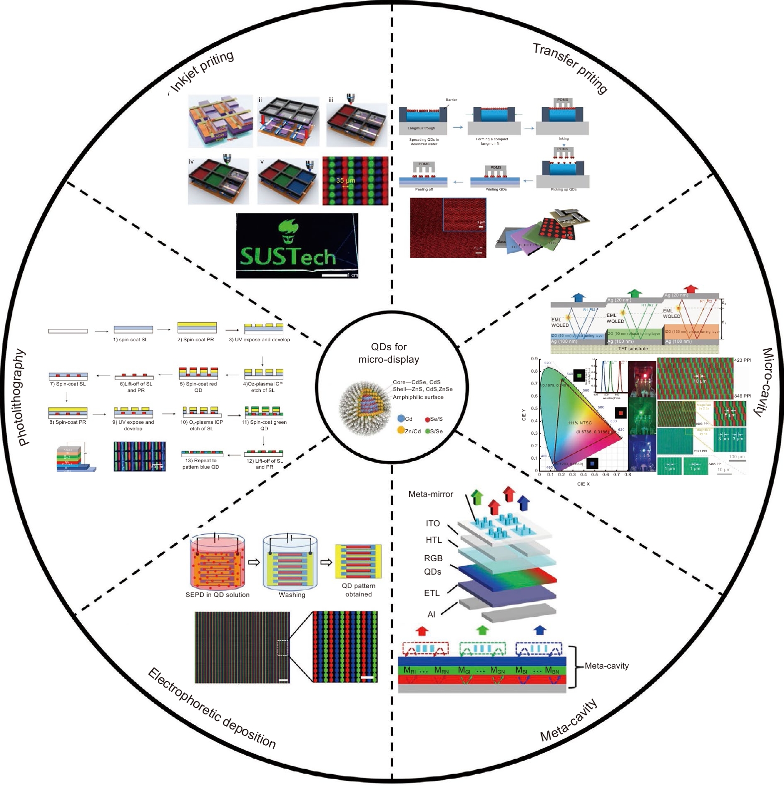
Overview: Quantum dot is a kind of semiconductor nanocrystal with a quantum confinement effect. Recently, quantum dots have been applied for display due to their advantages including high photoluminescent efficiency, tunable emission wavelength, narrow emission spectrum, and low-cost solution process. In this paper, we focus on the application of quantum dots in microdisplay. With the rising near-eye display demands such as AR/VR, the realization of full color, high efficiency, and high luminance microdisplay attracts many attentions. However, the realization of the target microdisplay is difficult due to the high-cost mass transfer technology in micro-LED and the insufficient luminance in micro-OLED. Here, the photoluminescent (PL) and electroluminescent (EL) quantum dots can provide new routes for microdisplay. For PL, quantum dots can work as color conversion material for micro-LED. The multiple-time mass transfer can be avoided with the combination of red and green quantum dots and blue micro-LED. Meanwhile, the color gamut can be improved due to the narrow FWHM of quantum dot emission. For EL, RGB quantum dots can work as an emission layer in QLED, and the RGB micro-QLED can be applied for microdisplay directly with a compact and high-efficiency system. Compared with OLED, the QLED can realize higher luminance due to the inherent stability of the inorganic quantum dot, which is more suitable for AR display requiring high luminance. The patterning of quantum dot layer is the first step for the application in microdisplay. For both PL and EL applications, a high pixel density, high pixel uniformity, high pixel consistency, and low-cost patterning method is required. For the quantum dot color conversion layer in PL application, a high optical density is required for the sufficient absorption of the blue light. For the quantum dot emission layer in EL application, the uniform and small roughness surface quantum dot layer is required with few damages to the quantum dots to ensure the good performance of QLED devices. There are several patterning methods have been reported for quantum dots including inkjet printing, photolithography, transfer printing, electrophoretic deposition, in situ fabrication, and optical micro cavity. However, it is still challenging to find a perfect patterning method for the quantum dot layer. For PL application, the stability of quantum dot under long time high-intensity blue light excitation is a big problem due to the photoinduced quenching and oxidation. For EL application, compared with red and green QLED, the peak luminance, efficiency, and lifetime of blue QLED needs to be further improved by optimizing the blue quantum dots and device structure to satisfy the requirement of the display application.
-

-
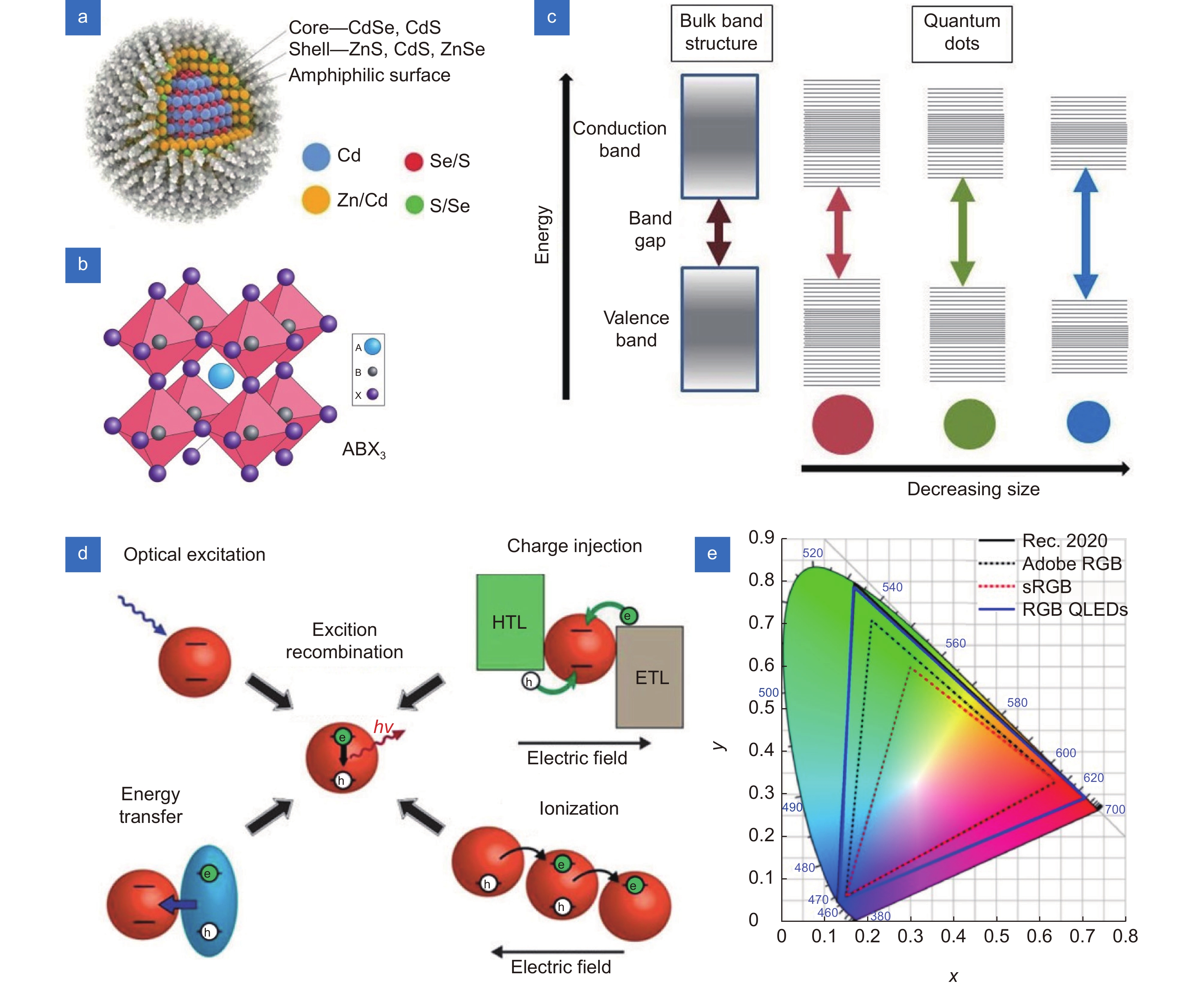
图 1 (a) 核壳结构胶体量子点示意图[20];(b) 钙钛矿纳米晶结构示意图[21];(c) 量子点尺寸与发光带隙的关系[22];(d) 量子点发光机理图[16]; (e) 基于红绿蓝三色量子点发光二极管的色域覆盖范围[17]
Figure 1. (a) Core-shell structure diagram of the colloidal quantum dot[20]; (b) Structure diagram of perovskite nanocrystal[21]; (c) Relationship between quantum dot size and emission bandgap[22]; (d) Excitation mechanisms of quantum dots[16]; (e) Color gamut representation of RGB QLEDs[17]
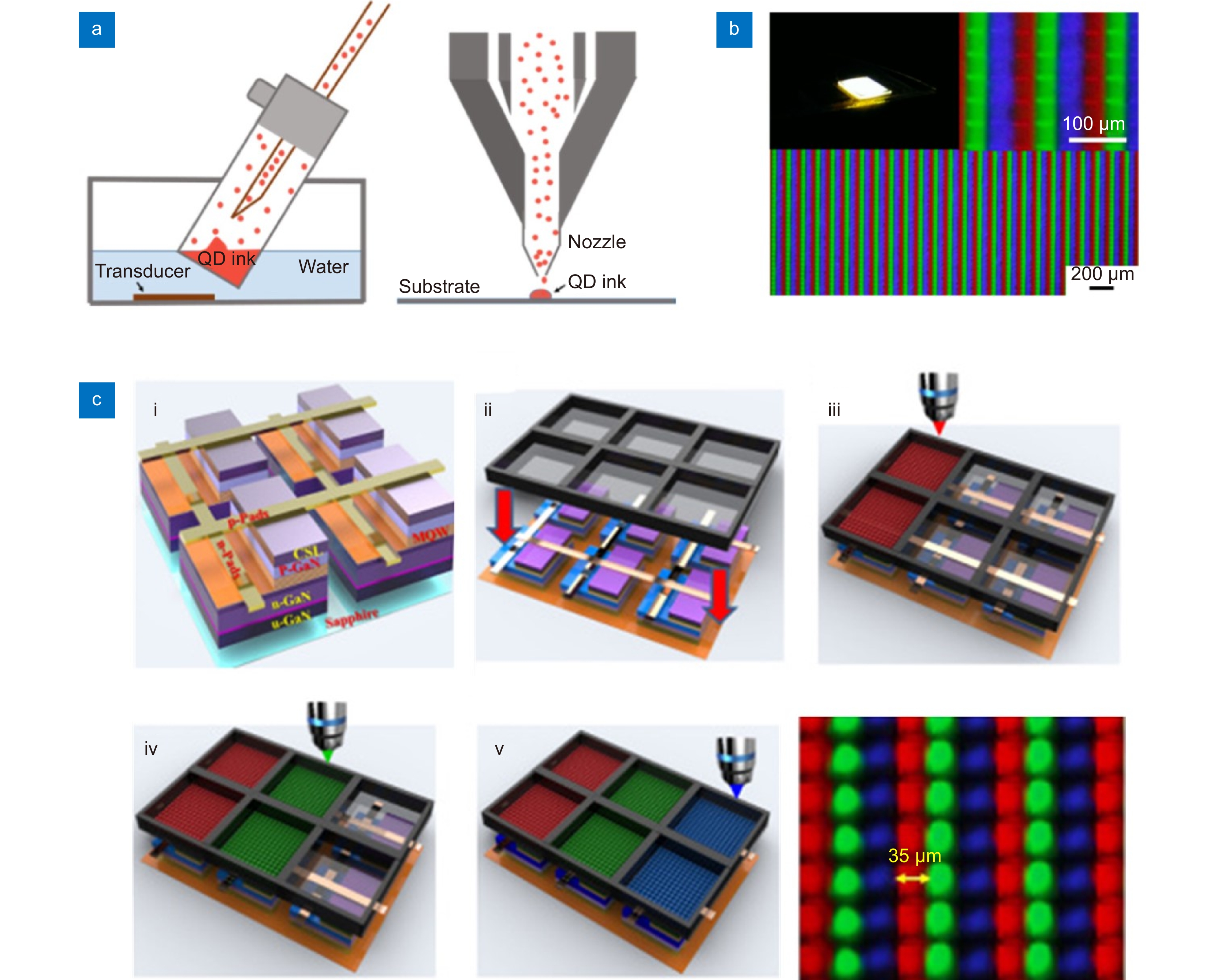
图 2 (a) 气溶胶喷印原理示意图; (b) 荧光显微镜下喷涂的量子点Micro-LED[30];(c) 气溶胶喷印基于量子点的全彩色Micro-LED的流程[31]
Figure 2. (a) The schematic diagram of the aerosol jet printing; (b) Full color quantum dots based Micro-LED image under fluorescence microscopy[30]; (c) The process of the full-color emission quantum dots based Micro-LED by aerosol jet printing[31]
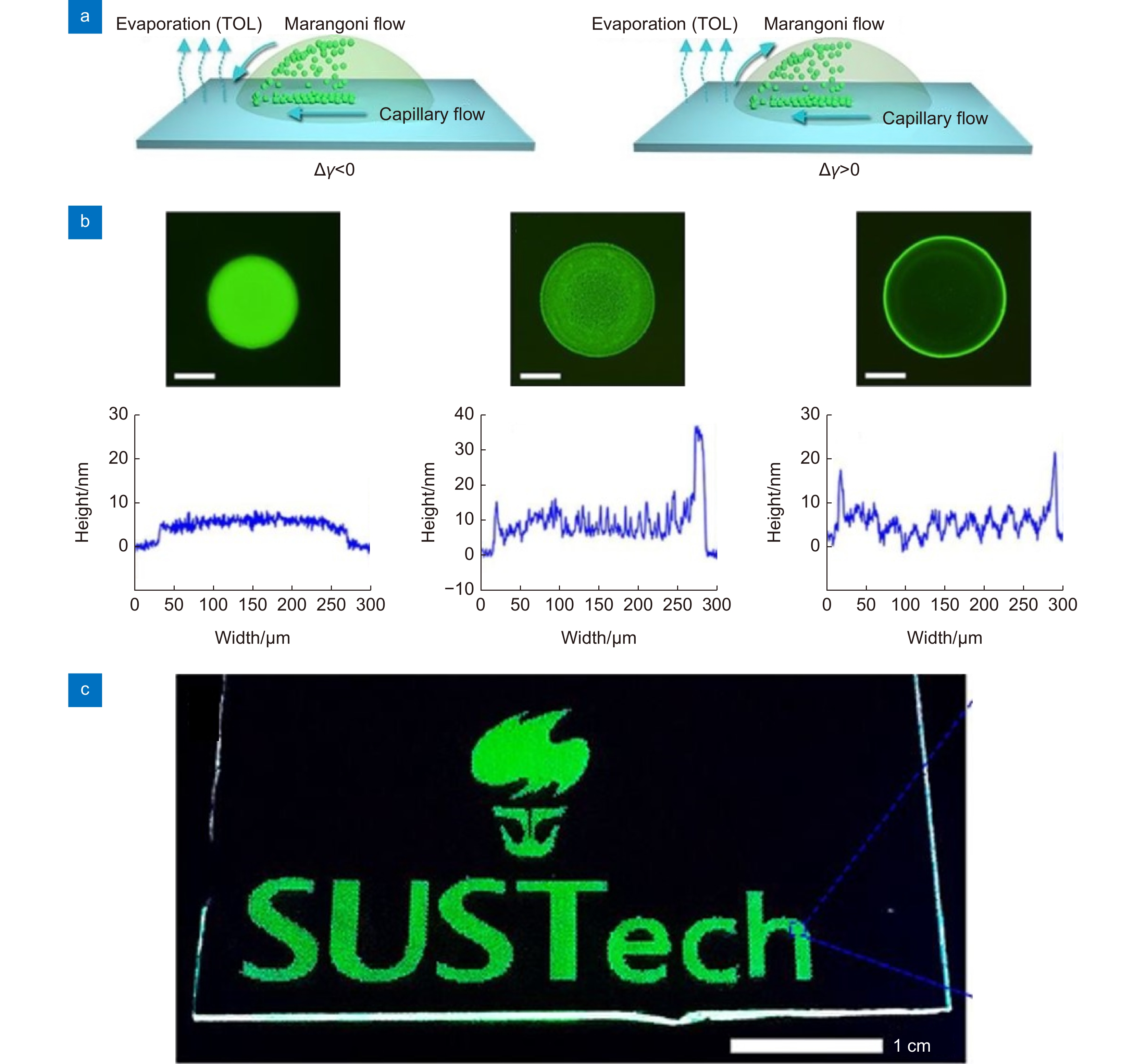
图 3 (a) 液滴干燥过程中的马朗戈尼流与毛细流示意图,左侧为液滴顶部区域表面张力小于边缘区域,右侧为液滴顶部区域表面张力大于边缘区域;(b) 荧光显微镜下十二烷占比60%、70%以及80%的墨滴以及其对应的表面形貌图。图中比例尺为100 μm;(c) 喷墨打印的CsPbBr3量子点图案[33]
Figure 3. (a) Schematic illustration of the marangoni flow and capillary flow: surface tension at the top area of the droplet is smaller than the edge(Δγ<0), and surface tension at the top of the droplet is larger than the edge area(Δγ>0); (b) Fluorescence image and corresponding surface profiles of the microarray with dodecane volume ratio of 60%, 70%, and 80% in the ink. The scale bars are 100 μm; (c) A CsPbBr3 quantum dot pattern by inkjet printing[33]
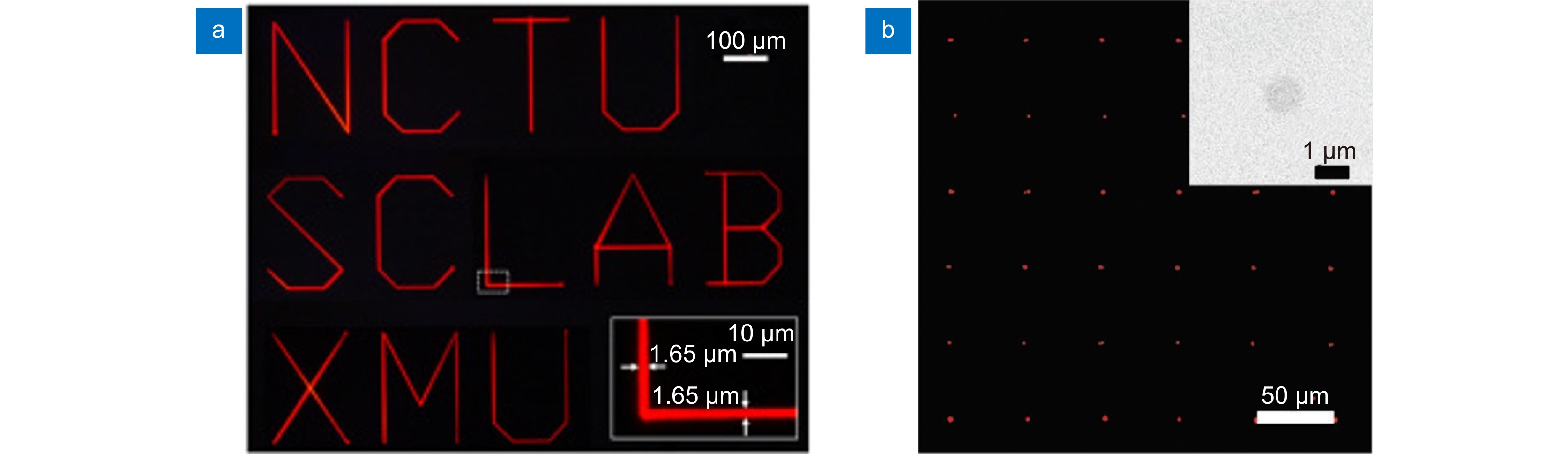
图 4 (a) 荧光显微镜下采用超精细喷墨打印系统在玻璃表面打印的红色量子点图案,最小线宽为1.65 μm[34];(b) 采用电流体喷印打印的红色量子点图案,直径为1 μm[35]
Figure 4. (a) Fluorescence microscope image of patterns printed on the glass by super-inkjet printing system, the minimum linewidth is 1.65 μm[34]; (b) Red quantum dot pattern by electrohydrodynamic printing with a diameter of 1 μm[35]
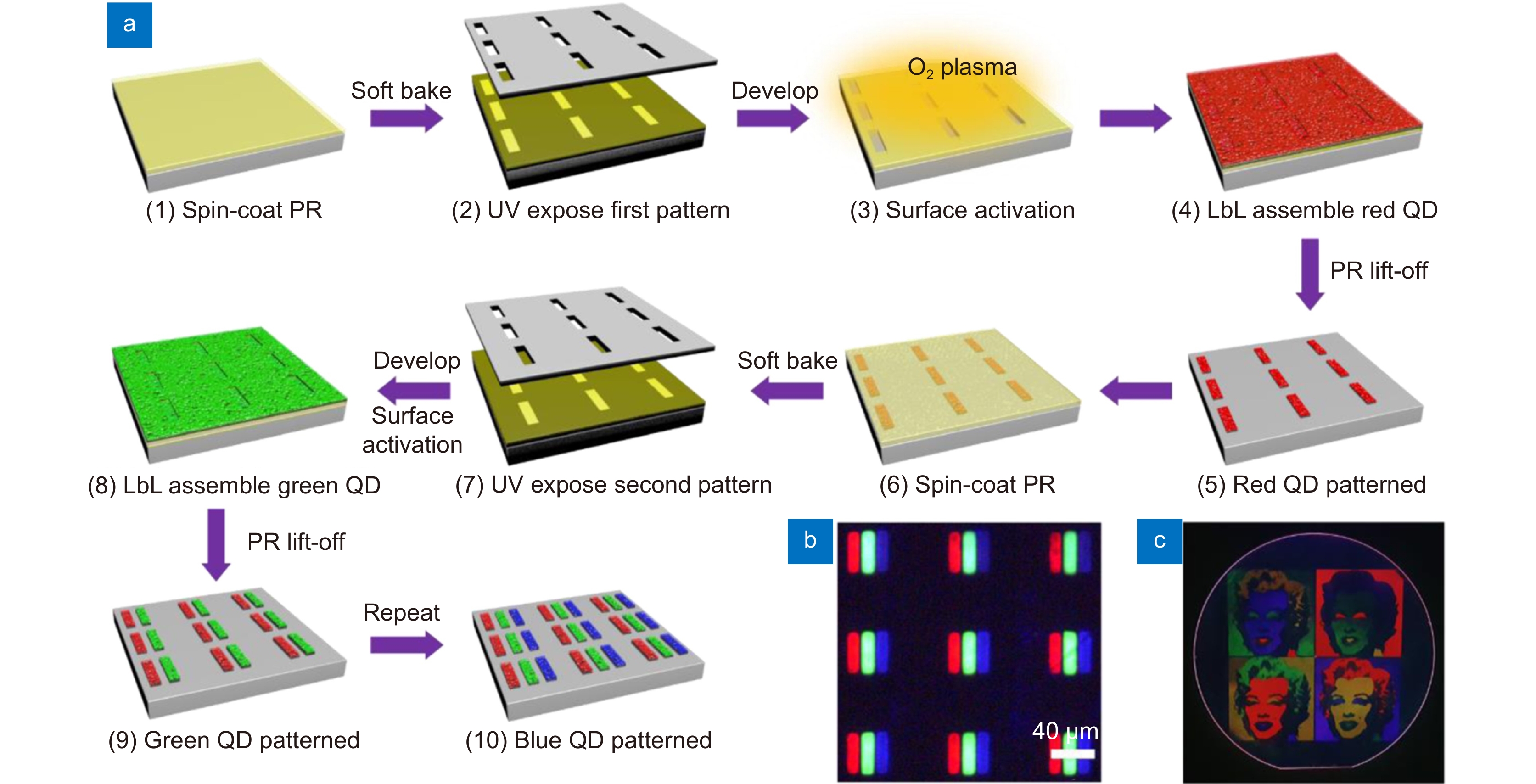
图 5 (a) 通过多次光刻进行量子点层图案化的制备流程; (b) 荧光显微镜(405 nm激光激发)下的图案化的红绿蓝量子点;(c) 紫外灯下4 inch石英晶圆的量子点图案展示图[36]
Figure 5. (a) Illustration of the quantum dot patterning by using repeated photolithography; (b) Microscope image of the patterned quantum dot under 405 nm laser excitation; (c) Large-scale quantum dot pattern demonstration on a 4 inch quartz wafer under UV lamp[36]
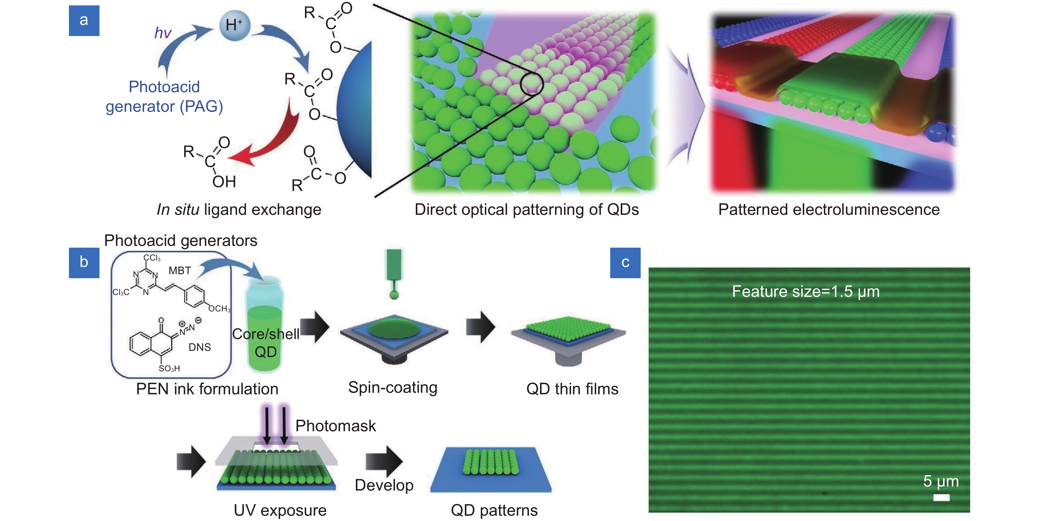
图 6 (a) 量子点直接光刻图案化的示意图; (b) 采用可光刻型墨水来制备图案化量子点的过程;(c) 荧光显微镜下绿色量子点图案,其最小线宽为1.5 μm[41]
Figure 6. (a) Schematic illustrations of the patterning concept of direct optical lithography of quantum dot; (b) Process of using photo-patternable emissive nanocrystal inks for patterning luminescent quantum dots; (c) Fluorescence optical microscopy images of green quantum dots pattern with a minimum line width of 1.5 μm[41]
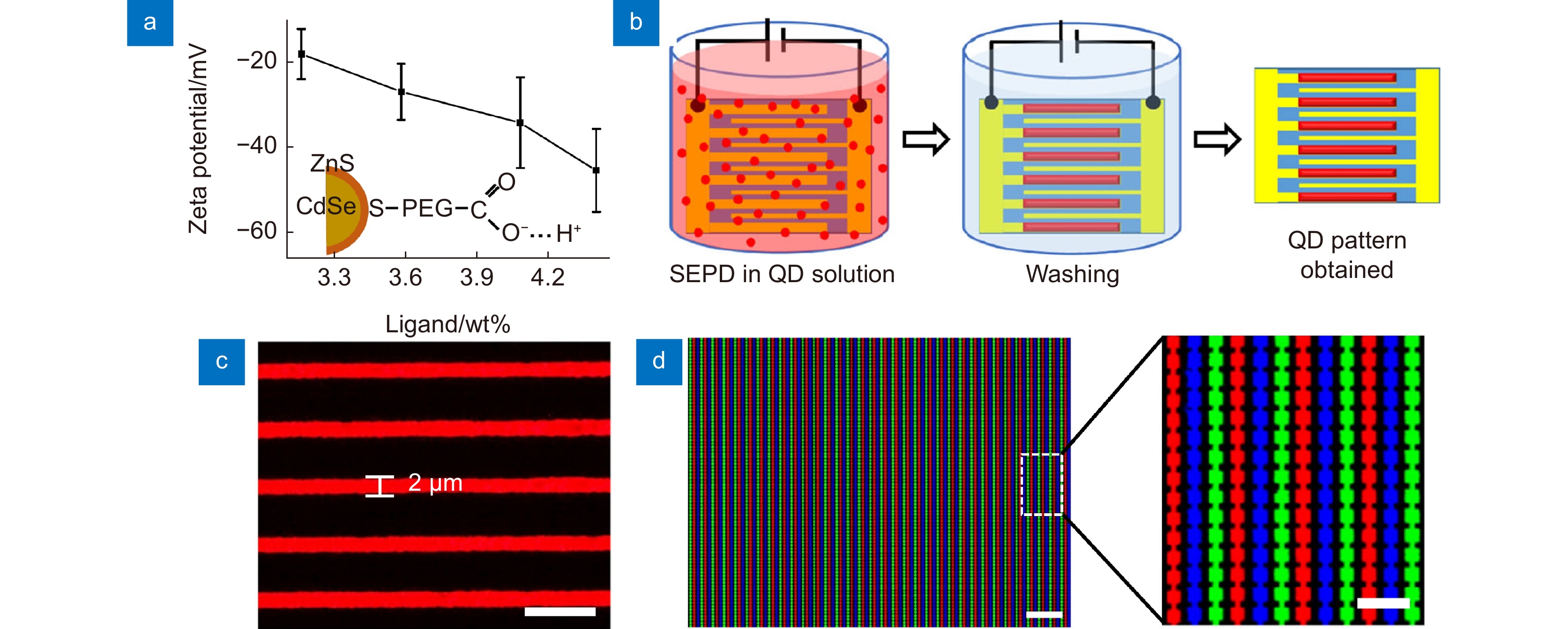
图 7 (a) 不同配体成分的量子点电动电势; (b) 通过电泳沉积法在预先制备的基板上沉积量子点的流程图;(c) 荧光显微镜下红色量子点条纹图,最小线宽为2 μm;(d) 荧光显微镜下通过三步选择性电泳沉积制备的红绿蓝量子点图案,左侧图中标尺为200 μm,右侧为50 μm[43]
Figure 7. (a) Zeta potentials of quantum dots capped with different ligand contents; (b) Schematic illustration of the quantum dots patterning process on the prefabricated substrate; (c) Fluorescence image of the red quantum dot stripe array with a line width of 2 μm. Scale bar: 10 μm; (d) Fluorescence images of RGB quantum dot patterns fabricated by three steps selective electrophoretic deposition. Scale bar: 200 μm(left) and 50 μm(right)[43]
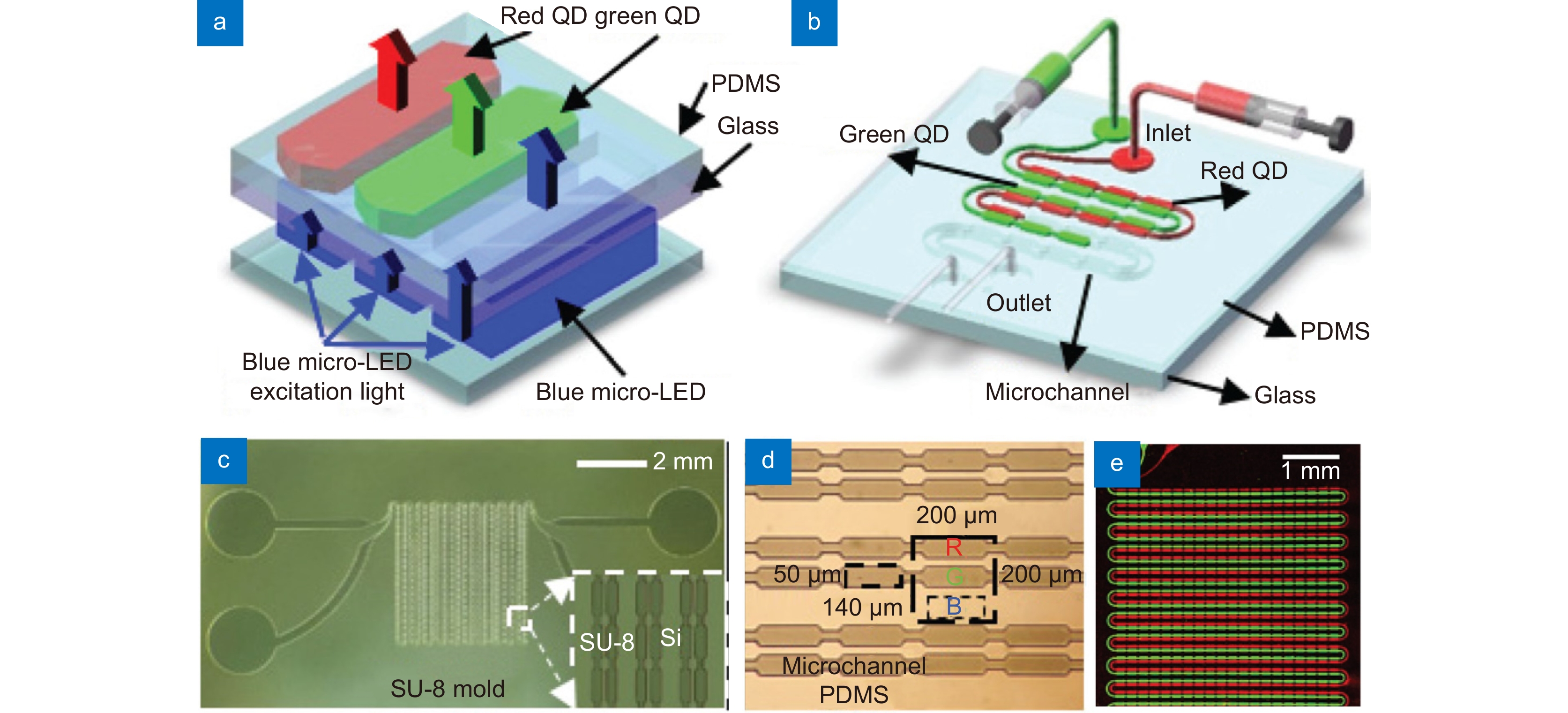
图 8 (a) 基于红绿量子点的全彩色Micro-LED显示像素单元示意图;(b) 通过注射器将红绿量子点注射进微流道的过程;(c) 硅片上SU-8模板; (d) 与玻璃基板粘合的PDMS微流道,子像素尺寸为50 μm×140 μm;(e) 200 μm尺寸的像素阵列量子点色转换层[44]
Figure 8. (a) Schematic diagram of a single pixel of the full color Micro-LED display based on red and green quantum dots; (b) Process of red and green quantum dots injection in the micro-channels; (c) SU-8 mold on the silicon substrate; (d) PDMS microchannel bond with the glass substrate with a sub pixel of 50 μm×140 μm; (e) Quantum dot color conversion layer with 200 μm full-color pixel pitches array[44]
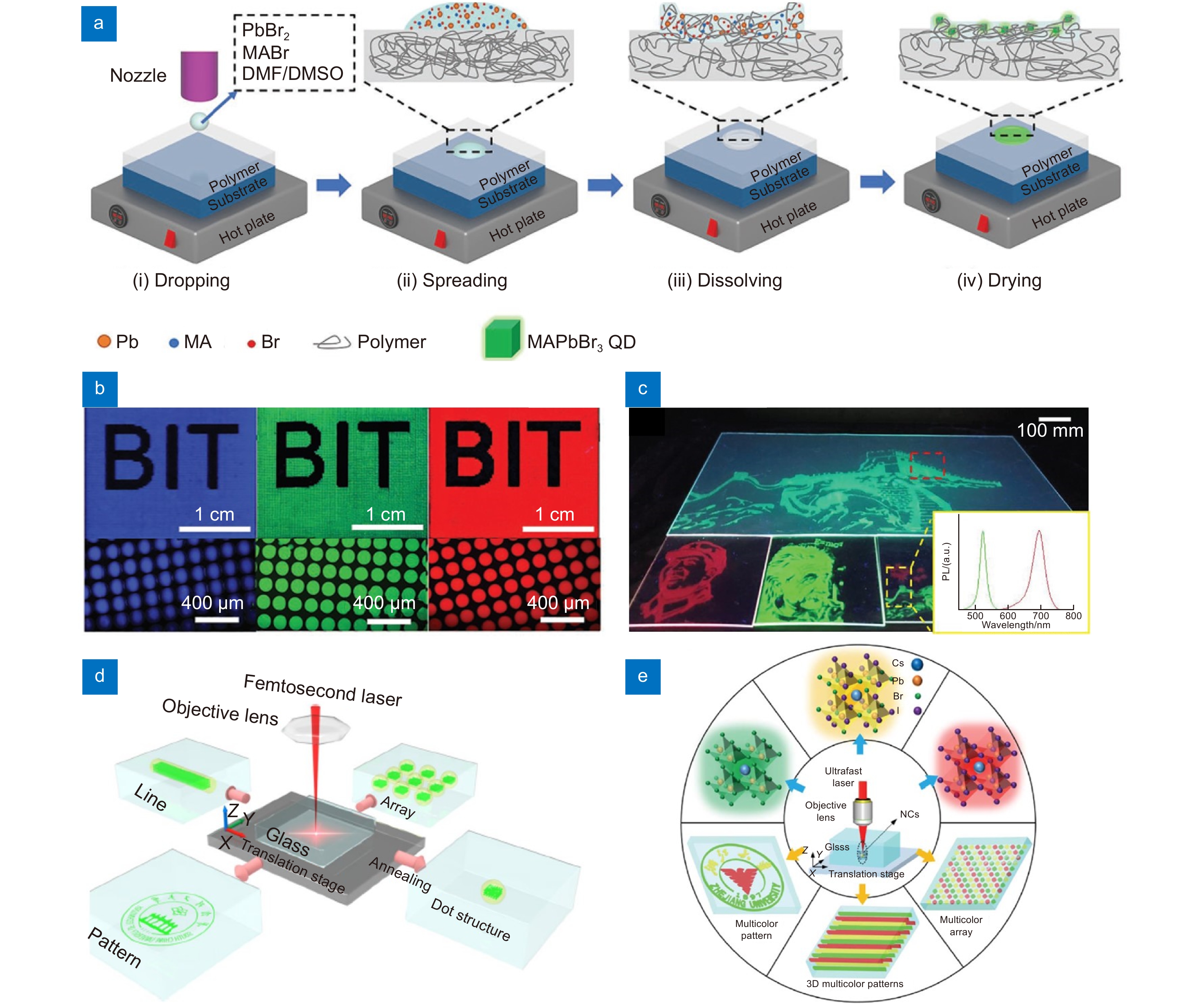
图 9 (a) 喷墨打印原位制备钙钛矿量子点流程图; (b) 紫外灯照射下的红绿蓝钙钛矿量子点图案[49];(c) 大面积图案化钙钛矿量子点层[51];(d) 激光直写原位制备钙钛矿量子点图案示意图[52];(e) 激光直写在玻璃内部制备不同颜色的钙钛矿量子点图案示意图[53]
Figure 9. (a) Schematic diagram of in situ inkjet printing strategy for fabricating patterning perovskite quantum dots patterns on polymer substrate; (b) Printed RGB perovskite quantum dots patterns under UV light illuminations[49]; (c) Photography of patterned perovskite-polymer composite sheets[51]; (d) In situ direct laser writing fabrication of perovskite quantum dots patterns inside of the glass[52]; (e) In situ direct laser writing fabrication of perovskite quantum dots with different colors inside of the glass[53]
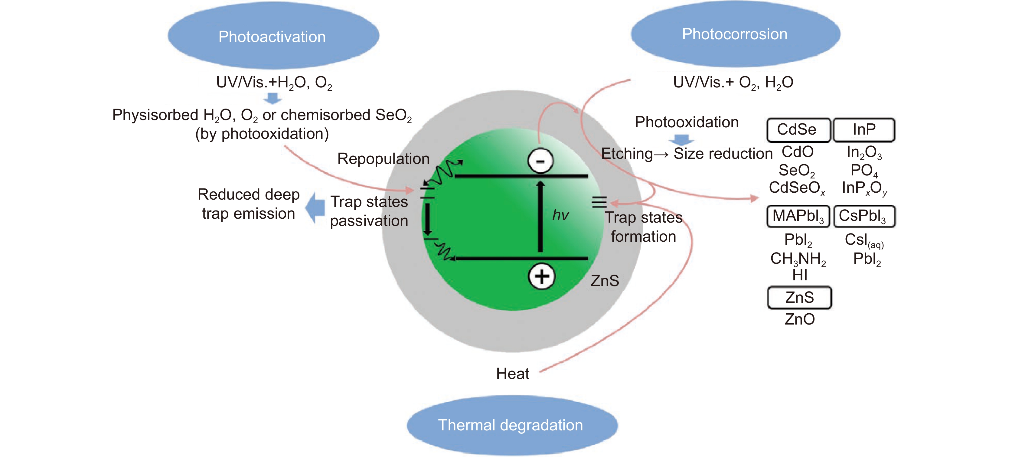

图 11 (a) QLED结构设计图;(b) QLED 能带结构图;(c) 电流体喷印示意图[35]; (d) 电流体喷印制备的量子点像素阵列;(e) 热退火后处理和梯度真空后处理墨滴干燥示意图; (f) 红光,(g) 绿光,以及(h) 蓝光的喷墨打印(圆点)和旋涂(方点)QLED外量子效率-亮度特性。插图标尺为5 cm[59]
Figure 11. (a) Structure design of the QLED devices; (b) Energy level diagram of the QLED; (c) Schematic of electrohydrodynamic printing to fill the pixel on the substrate[35]; (d) The fluorescent microphotograph of high-resolution pixels by electrohydrodynamic printing; (e) The scheme of droplet evaporation processes for heat post-treatment (HP) and gradient vacuum post-treatment (GVP) methods. EQE-luminance curves of (f) red, (g) green, and (h) blue inkjet printing(circle) and spin-coating(square) QLED. The scale bar is 5 cm in the insert picture[49]
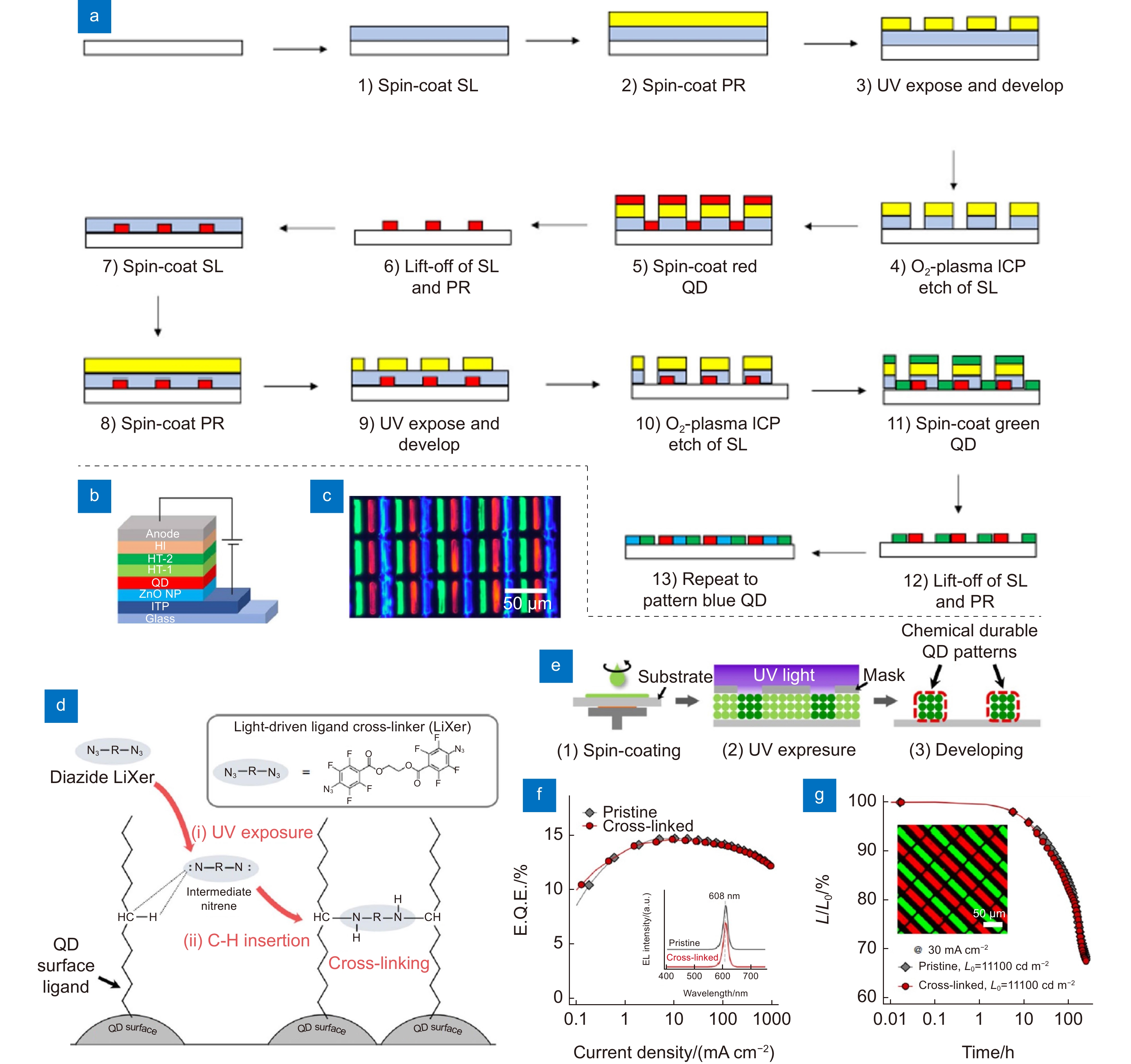
图 12 (a) 牺牲层辅助光刻制备多色量子点图案流程图; (b) Micro-QLED器件结构示意图; (c) 500 ppi的Micro-QLED电致发光图[37]; (d) 邻近量子点配体基于C-H键间的反应发生交联的示意图;(e) 使用LiXer的量子点光刻流程图;(f) 发生交联的和未发生交联的QLED外量子效率-电流曲线;(g) 发生交联的和未发生交联的QLED寿命测试(初始亮度为11000 尼特,插图中子像素大小为10 μm×38 μm) [42]
Figure 12. (a) Schematic illustration of patterning QDs with different color on a substrate via scarify layer assisted photolithography approach; (b) The device structure of Micro-QLED; (c) The electroluminescent image of the 500 ppi full-color Micro-QLED array[37]; (d) Schematic description of the ligand crosslinking process between neighboring quantum dots based on the C-H insertion reaction of the nitrene moiety of LiXer; (e) Schematic description of the photo-patterning processes of quantum dots using LiXer; (f) External quantum efficiency (EQE) – current density characteristics of pristine and cross-linked QLED devices; (g) Lifetime measurement of pristine and cross-linked QLED devices with an initial luminance of 11000 cd/m2. The sub pixel size in the inset image is 10 μm×38 μm[42]
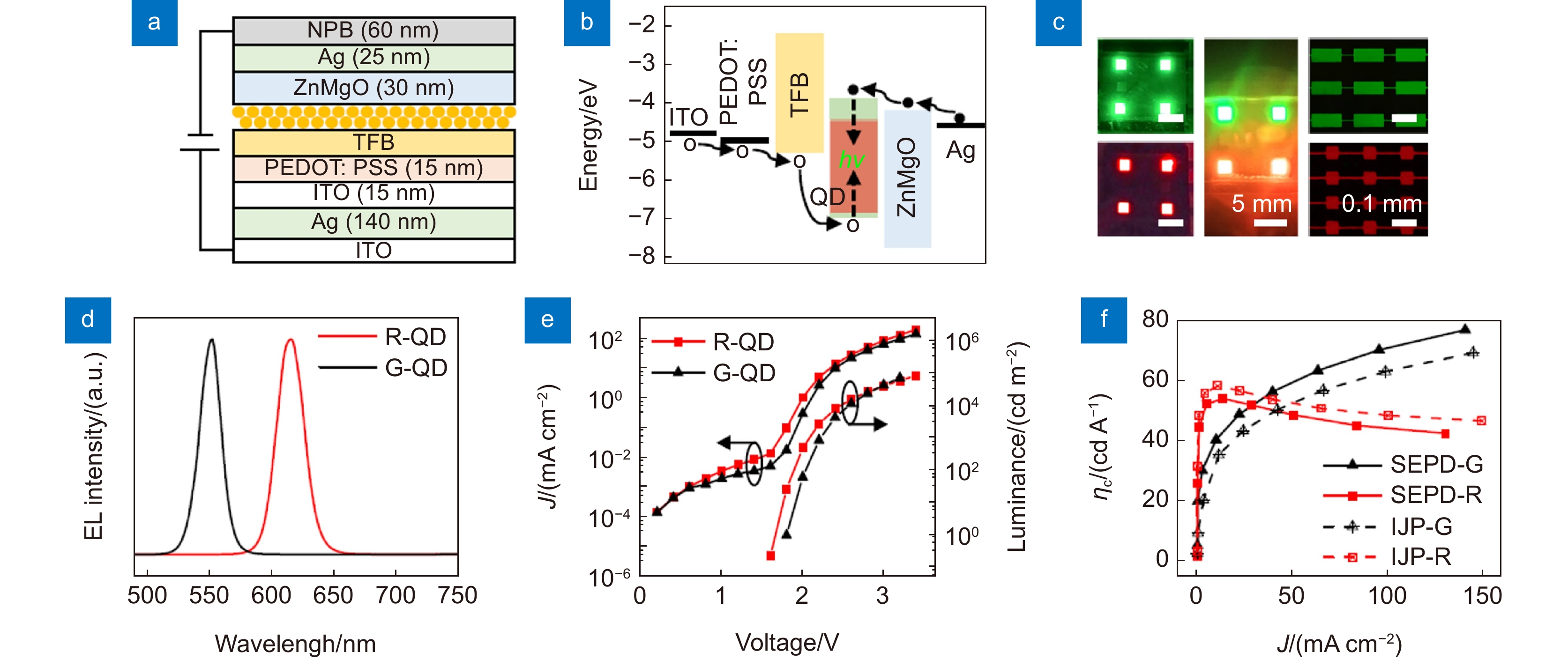
图 13 电泳沉积法制备的QLED光电特性。(a) QLED器件结构示意图;(b) QLED器件能带示意图;(c) QLED像素电致发光图; (d) 红绿QLED发光光谱图;(e) 红绿QLED电流密度 – 亮度 – 电压特征曲线图;(f) 红绿QLED电流效率 – 电流密度特征曲线图[43]
Figure 13. Optoelectronics properties of QLED by selective electrophoretic deposition.(a) Schematic diagram of the device structure of SEPD processed QLEDs; (b) Energy band diagram of the QLEDs; (c) Image of red and green SEPD QLED pixels. Scale bar: 5 mm and 0.1 mm; (d) Normalized electroluminescent spectra of red and green SEPD QLEDs; (e) Current density - luminance - voltage (J-L-V) characteristics of the red and green SEPD QLEDs; (f) Current efficiency - current density of SEPD QLED (solid line)[43]
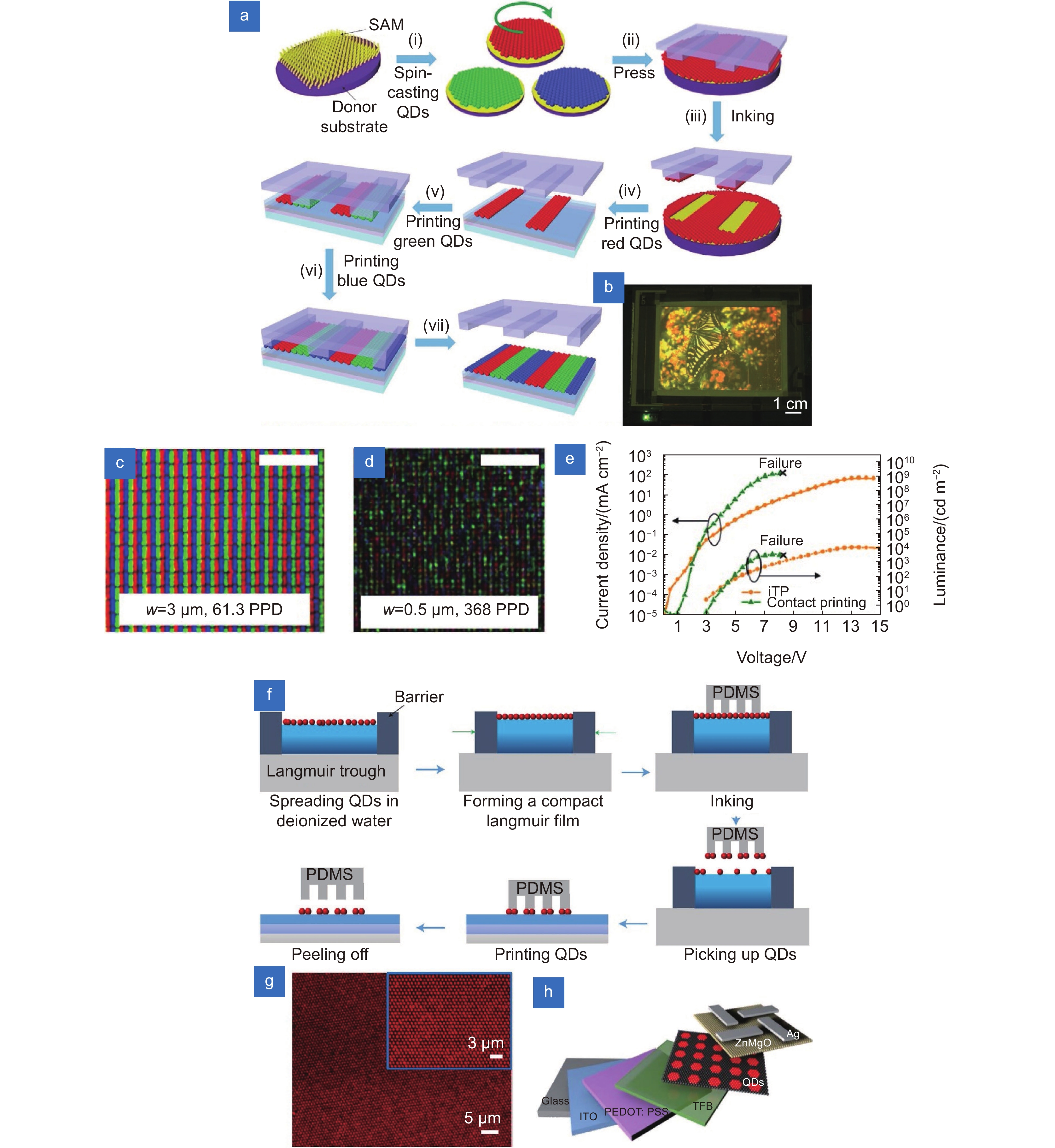
图 14 转印技术制备Micro-QLED。(a) 采用转印技术图案化量子点的过程;(b) 4 inch全彩色量子点图像显示器,分辨率为320×240[60]; 共聚焦显微镜下红绿蓝三色的量子点像素化阵列,子像素宽度为(c) 3 μm以及(d) 0.5 μm; (e) 浸没式转印(黄线)和接触式印刷(绿线)制备的器件电流密度-电压-亮度特征曲线[61];(f) LB-转印技术制备图案化量子点流程图;(g) 荧光显微镜下红光量子点图案;(h) 图案化红光Micro-QLED器件结构图 [62]
Figure 14. Micro-QLED by transfer printing.(a) Schematic of transfer printing process for patterning of quantum dots; (b) Electroluminescence image of a 4-inch full-color quantum dot display with a resolution of 320×240[60]; Confocal fluorescence images of full-color RGB quantum dots arrays with subpixel width of (c) 3 μm and (d) 0.5 μm; (e) Current density–voltage–luminance (J–V–L) characteristics of immersion transfer printing (yellow line) and contact printing (green line) devices[61]; (f) Schematic of the langmuir-Blodgett method assisted transfer printing process; (g) Fluorescence microscopy image of patterned red-QD-film arrays with scale bar of 5 μm and 3 μm (insert picture); (h) Schematic of the patterned red micro-QLED [62]

图 15 光学谐振腔方案实现全彩色Micro-QLED[66]。(a) 器件结构示意图;(b) 基于微腔的红绿蓝QLED工作原理示意图;(c) 红绿蓝三色QLED色坐标图;(d) 像素化的QLED阵列,方块型像素大小从10 µm到5 µm,条纹状像素宽度从3 µm到1 µm
Figure 15. Realization of full color Micro-QLED by optical resonant cavity[66]. (a) Schematic device structure of QLED; (b) Working principle of RGB micro-cavity based QLED; (c) The color coordinates and color triangle of the converted red, green, and blue emission. The color gamut can achieve 110% NTSC; (d) Pixelated QLED arrays with square pixel shape and subpixel size from 10 µm to 5 µm, and line shape with subpixel size from 3 µm to 1 µm
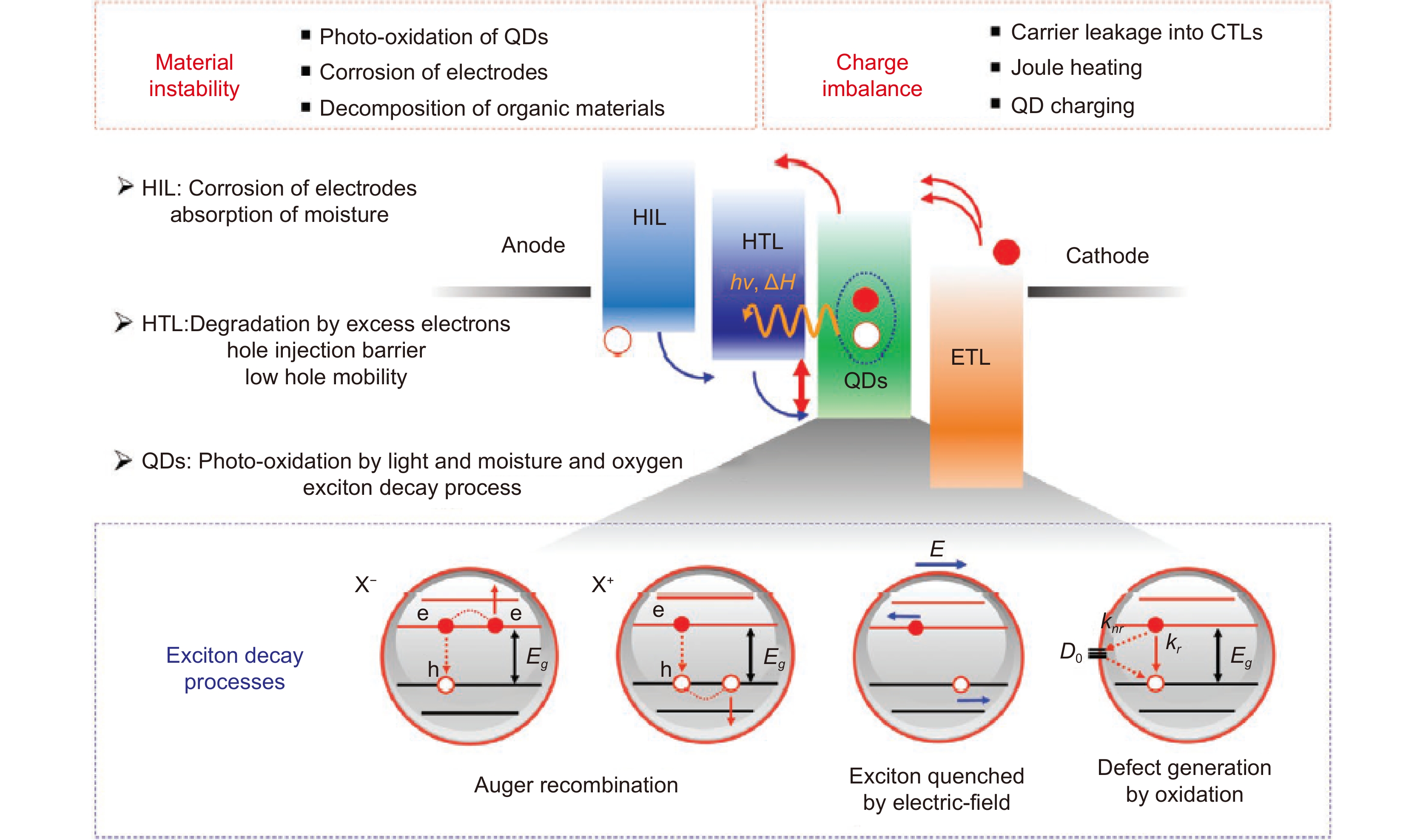
表 1 各种量子点图案化方式对比
Table 1. Comparison between different patterning methods for quantum dots
图案化方式 应用范围 最小图案尺寸/μm 常规尺寸(~mm)QLED器件性能 参考文献 最高亮度/nit 外量子效率/(%) 电流效率/(cd/A) 喷印技术 光致/电致 1 8533(R) 0.55 / [35] / 104826(R)
283996(G)
2367(B)19.3(R)
18.0(G)
4.4(B)/ [59] 光刻技术 光致/电致 5 108000(R)
247000(G)
304(B)/ 8.3(R)
9.8(G)
0.02(B)[37] 1.5 22500 (G) 5.08 12.92 [41] 转移印刷 光致/电致 0.5 10711(G) 3.3 14.8 [61] 1 262400(R) 14.7 20.2 [62] 电泳沉积 光致/电致 2 79489(R)
67111(G)/ 54.2(R)
77.0(G)[43] 微流道 光致 50 / / / [44] 原位制备 光致 0.9 / / / [50] 光学微腔 电致 1 22170(R)
51930(G)
3064 (B)/ 25.2(R)
17.2(G)
0.99(B)[66]  下载: 导出CSV
-
[1] Cheng D W, Wang Q W, Liu Y, et al. Design and manufacture AR head-mounted displays: A review and outlook[J]. Light Adv Manuf, 2021, 2(3): 24. doi: 10.37188/lam.2021.024
[2] Algorri J F, Del Pozo V U, Sańchez-Pena J M, et al. An autostereoscopic device for mobile applications based on a liquid crystal microlens array and an OLED display[J]. J Disp Technol, 2014, 10(9): 713−720. doi: 10.1109/JDT.2014.2313143
[3] Huang Y G, Hsiang E L, Deng M Y, et al. Mini-LED, micro-LED and OLED displays: present status and future perspectives[J]. Light Sci Appl, 2020, 9: 105. doi: 10.1038/s41377-020-0341-9
[4] Lee V W, Twu N, Kymissis I. Micro-LED technologies and applications[J]. Inf Disp, 2016, 32(6): 16−23.
[5] Wu T Z, Sher C W, Lin Y, et al. Mini-LED and micro-LED: promising candidates for the next generation display technology[J]. Appl Sci, 2018, 8(9): 1557. doi: 10.3390/app8091557
[6] Huang Y G, Tan G J, Gou F W, et al. Prospects and challenges of mini-LED and micro-LED displays[J]. J Soc Inf Disp, 2019, 27(7): 387−401. doi: 10.1002/jsid.760
[7] Liu Z J, Lin C H, Hyun B R, et al. Micro-light-emitting diodes with quantum dots in display technology[J]. Light Sci Appl, 2020, 9: 83. doi: 10.1038/s41377-020-0268-1
[8] Bera D, Qian L, Tseng T K, et al. Quantum dots and their multimodal applications: a review[J]. Materials, 2010, 3(4): 2260−2345. doi: 10.3390/ma3042260
[9] Vasudevan D, Gaddam R R, Trinchi A, et al. Core–shell quantum dots: properties and applications[J]. J Alloys Compd, 2015, 636: 395−404. doi: 10.1016/j.jallcom.2015.02.102
[10] Dai X L, Deng Y Z, Peng X G, et al. Quantum-dot light-emitting diodes for large-area displays: towards the dawn of commercialization[J]. Adv Mater, 2017, 29(14): 1607022. doi: 10.1002/adma.201607022
[11] Tan Z K, Moghaddam R S, Lai M L, et al. Bright light-emitting diodes based on organometal halide perovskite[J]. Nat Nanotechnol, 2014, 9(9): 687−692. doi: 10.1038/nnano.2014.149
[12] Wang H C, Bao Z, Tsai H Y, et al. Perovskite quantum dots and their application in light-emitting diodes[J]. Small, 2018, 14(1): 1702433. doi: 10.1002/smll.201702433
[13] Van Le Q, Hong K, Jang H W, et al. Halide perovskite quantum dots for light-emitting diodes: properties, synthesis, applications, and outlooks[J]. Adv Electron Mater, 2018, 4(12): 1800335. doi: 10.1002/aelm.201800335
[14] Chen D Q, Chen X. Luminescent perovskite quantum dots: synthesis, microstructures, optical properties and applications[J]. J Mater Chem C, 2019, 7(6): 1413−1446. doi: 10.1039/C8TC05545A
[15] Miao Y F, Ke Y, Wang N N, et al. Stable and bright formamidinium-based perovskite light-emitting diodes with high energy conversion efficiency[J]. Nat Commun, 2019, 10(1): 3624. doi: 10.1038/s41467-019-11567-1
[16] Supran G J, Shirasaki Y, Song K W, et al. QLEDs for displays and solid-state lighting[J]. MRS Bull, 2013, 38(9): 703−711. doi: 10.1557/mrs.2013.181
[17] Zhu R D, Luo Z Y, Chen H W, et al. Realizing Rec. 2020 color gamut with quantum dot displays[J]. Opt Express, 2015, 23(18): 23680−23693. doi: 10.1364/OE.23.023680
[18] Liu Z J, Hyun B R, Sheng Y J, et al. Micro-light-emitting diodes based on InGaN materials with quantum dots[J]. Adv Mater Technol, 2022, 7(6): 2101189. doi: 10.1002/admt.202101189
[19] Fan X T, Wu T Z, Liu B, et al. Recent developments of quantum dot based micro-LED based on non-radiative energy transfer mechanism[J]. Opto-Electron Adv, 2021, 4(4): 210022. doi: 10.29026/oea.2021.210022
[20] Nasirzadeh K, Nazarian S, Hayat S M G. Inorganic nanomaterials: a brief overview of the applications and developments in sensing and drug delivery[J]. J Appl Biotechnol Rep, 2016, 3(2): 395−402.
[21] Green M A, Ho-Baillie A, Snaith H J. The emergence of perovskite solar cells[J]. Nat Photonics, 2014, 8(7): 506−514. doi: 10.1038/nphoton.2014.134
[22] Hong N H. Introduction to nanomaterials: basic properties, synthesis, and characterization[M]//Hong N H. Nano-Sized Multifunctional Materials. Amsterdam: Elsevier, 2019: 1–19.
[23] Feng F, Zhang K, Liu Y B, et al. AlGaN-based deep-UV micro-LED array for quantum dots converted display with ultra-wide color gamut[J]. IEEE Electron Device Lett, 2022, 43(1): 60−63. doi: 10.1109/LED.2021.3130750
[24] Singh M, Haverinen H M, Dhagat P, et al. Inkjet printing-process and its applications[J]. Adv Mater, 2010, 22(6): 673−685. doi: 10.1002/adma.200901141
[25] Lan L H, Zou J H, Jiang C B, et al. Inkjet printing for electroluminescent devices: emissive materials, film formation, and display prototypes[J]. Front Optoelectron, 2017, 10(4): 329−352. doi: 10.1007/s12200-017-0765-x
[26] Liu Y, Li F S, Xu Z W, et al. Efficient all-solution processed quantum dot light emitting diodes based on inkjet printing technique[J]. ACS Appl Mater Interfaces, 2017, 9(30): 25506−25512. doi: 10.1021/acsami.7b05381
[27] Yang P H, Zhang L, Kang D J, et al. High-resolution inkjet printing of quantum dot light-emitting microdiode arrays[J]. Adv Opt Mater, 2020, 8(1): 1901429. doi: 10.1002/adom.201901429
[28] Hu Z P, Yin Y M, Ali M U, et al. Inkjet printed uniform quantum dots as color conversion layers for full-color OLED displays[J]. Nanoscale, 2020, 12(3): 2103−2110. doi: 10.1039/C9NR09086J
[29] Zheng C B, Zheng X, Feng C, et al. High-brightness perovskite quantum dot light-emitting devices using inkjet printing[J]. Org Electron, 2021, 93: 106168. doi: 10.1016/j.orgel.2021.106168
[30] Han H V, Lin H Y, Lin C C, et al. Resonant-enhanced full-color emission of quantum-dot-based micro LED display technology[J]. Opt Express, 2015, 23(25): 32504−32515. doi: 10.1364/OE.23.032504
[31] Lin H Y, Sher C W, Hsieh D H, et al. Optical cross-talk reduction in a quantum-dot-based full-color micro-light-emitting-diode display by a lithographic-fabricated photoresist mold[J]. Photonics Res, 2017, 5(5): 411−416. doi: 10.1364/PRJ.5.000411
[32] Li Y, Chen Z W, Liang D, et al. Coffee-stain-free perovskite film for efficient printed light-emitting diode[J]. Adv Opt Mater, 2021, 9(17): 2100553. doi: 10.1002/adom.202100553
[33] Gao A J, Yan J, Wang Z J, et al. Printable CsPbBr3 perovskite quantum dot ink for coffee ring-free fluorescent microarrays using inkjet printing[J]. Nanoscale, 2020, 12(4): 2569−2577. doi: 10.1039/C9NR09651E
[34] Chen S W H, Shen C C, Wu T Z, et al. Full-color monolithic hybrid quantum dot nanoring micro light-emitting diodes with improved efficiency using atomic layer deposition and nonradiative resonant energy transfer[J]. Photonics Res, 2019, 7(4): 416−422. doi: 10.1364/PRJ.7.000416
[35] Li H G, Duan Y Q, Shao Z L, et al. High-resolution pixelated light emitting diodes based on electrohydrodynamic printing and coffee-ring-free quantum dot film[J]. Adv Mater Technol, 2020, 5(10): 2000401. doi: 10.1002/admt.202000401
[36] Park J S, Kyhm J, Kim H H, et al. Alternative patterning process for realization of large-area, full-color, active quantum dot display[J]. Nano Lett, 2016, 16(11): 6946−6953. doi: 10.1021/acs.nanolett.6b03007
[37] Mei W H, Zhang Z Q, Zhang A D, et al. High-resolution, full-color quantum dot light-emitting diode display fabricated via photolithography approach[J]. Nano Res, 2020, 13(9): 2485−2491. doi: 10.1007/s12274-020-2883-9
[38] Kim H M, Ryu M, Cha J H J, et al. Ten micrometer pixel, quantum dots color conversion layer for high resolution and full color active matrix micro-LED display[J]. J Soc Inf Disp, 2019, 27(6): 347−353. doi: 10.1002/jsid.782
[39] Li X H, Kundaliya D, Tan Z J, et al. Projection lithography patterned high-resolution quantum dots/thiol-ene photo-polymer pixels for color down conversion[J]. Opt Express, 2019, 27(21): 30864−30874. doi: 10.1364/OE.27.030864
[40] Zhao B X, Zhang X L, Bai X, et al. Surface modification toward luminescent and stable silica-coated quantum dots color filter[J]. Sci China Mater, 2019, 62(10): 1463−1469. doi: 10.1007/s40843-019-9435-7
[41] Cho H, Pan J A, Wu H Q, et al. Direct optical patterning of quantum dot light-emitting diodes via in situ ligand exchange[J]. Adv Mater, 2020, 32(46): 2003805. doi: 10.1002/adma.202003805
[42] Yang J, Hahm D, Kim K, et al. High-resolution patterning of colloidal quantum dots via non-destructive, light-driven ligand crosslinking[J]. Nat Commun, 2020, 11(1): 2874. doi: 10.1038/s41467-020-16652-4
[43] Zhao J Y, Chen L X, Li D Z, et al. Large-area patterning of full-color quantum dot arrays beyond 1000 pixels per inch by selective electrophoretic deposition[J]. Nat Commun, 2021, 12(1): 4603. doi: 10.1038/s41467-021-24931-x
[44] Li Y, Tao J, Wang Q, et al. Microfluidics-based quantum dot color conversion layers for full-color micro-LED display[J]. Appl Phys Lett, 2021, 118(17): 173501. doi: 10.1063/5.0047854
[45] Protesescu L, Yakunin S, Bodnarchuk M I, et al. Nanocrystals of cesium lead halide perovskites (CsPbX3, X = Cl, Br, and I): novel optoelectronic materials showing bright emission with wide color gamut[J]. Nano Lett, 2015, 15(6): 3692−3696. doi: 10.1021/nl5048779
[46] Stoumpos C C, Kanatzidis M G. Halide perovskites: poor man's high-performance semiconductors[J]. Adv Mater, 2016, 28(28): 5778−5793. doi: 10.1002/adma.201600265
[47] Veldhuis S A, Boix P P, Yantara N, et al. Perovskite materials for light-emitting diodes and lasers[J]. Adv Mater, 2016, 28(32): 6804−6834. doi: 10.1002/adma.201600669
[48] Li Z T, Cao K, Li J S, et al. Review of blue perovskite light emitting diodes with optimization strategies for perovskite film and device structure[J]. Opto-Electron Adv, 2021, 4(2): 200019. doi: 10.29026/oea.2021.200019
[49] Shi L F, Meng L H, Jiang F, et al. In situ inkjet printing strategy for fabricating perovskite quantum dot patterns[J]. Adv Funct Mater, 2019, 29(37): 1903648. doi: 10.1002/adfm.201903648
[50] Zhan W J, Meng L H, Shao C D, et al. In situ patterning perovskite quantum dots by direct laser writing fabrication[J]. ACS Photonics, 2021, 8(3): 765−770. doi: 10.1021/acsphotonics.1c00118
[51] Jia S Q, Li G Y, Liu P, et al. Highly luminescent and stable green quasi-2D perovskite-embedded polymer sheets by inkjet printing[J]. Adv Funct Mater, 2020, 30(24): 1910817. doi: 10.1002/adfm.201910817
[52] Huang X J, Guo Q Y, Yang D D, et al. Reversible 3D laser printing of perovskite quantum dots inside a transparent medium[J]. Nat Photonics, 2020, 14(2): 82−88. doi: 10.1038/s41566-019-0538-8
[53] Sun K, Tan D Z, Fang X Y, et al. Three-dimensional direct lithography of stable perovskite nanocrystals in glass[J]. Science, 2022, 375(6578): 307−310. doi: 10.1126/science.abj2691
[54] Moon H, Lee C, Lee W, et al. Stability of quantum dots, quantum dot films, and quantum dot light-emitting diodes for display applications[J]. Adv Mater, 2019, 31(34): 1804294. doi: 10.1002/adma.201804294
[55] Chang J H, Park P, Jung H, et al. Unraveling the origin of operational instability of quantum dot based light-emitting diodes[J]. ACS Nano, 2018, 12(10): 10231−10239. doi: 10.1021/acsnano.8b03386
[56] Chen S, Cao W R, Liu T L, et al. On the degradation mechanisms of quantum-dot light-emitting diodes[J]. Nat Commun, 2019, 10(1): 765. doi: 10.1038/s41467-019-08749-2
[57] Rhee S, Kim K, Roh J, et al. Recent progress in high-luminance quantum dot light-emitting diodes[J]. Curr Opt Photonics, 2020, 4(3): 161−173.
[58] Sun Y Z, Su Q, Zhang H, et al. Investigation on thermally induced efficiency roll-off: toward efficient and ultrabright quantum-dot light-emitting diodes[J]. ACS Nano, 2019, 13(10): 11433−11442. doi: 10.1021/acsnano.9b04879
[59] Jia S Q, Tang H D, Ma J R, et al. High performance inkjet-printed quantum-dot light-emitting diodes with high operational stability[J]. Adv Opt Mater, 2021, 9(22): 2101069. doi: 10.1002/adom.202101069
[60] Kim T H, Cho K S, Lee E K, et al. Full-colour quantum dot displays fabricated by transfer printing[J]. Nat Photonics, 2011, 5(3): 176−182. doi: 10.1038/nphoton.2011.12
[61] Nam T W, Kim M, Wang Y M, et al. Thermodynamic-driven polychromatic quantum dot patterning for light-emitting diodes beyond eye-limiting resolution[J]. Nat Commun, 2020, 11(1): 3040. doi: 10.1038/s41467-020-16865-7
[62] Meng T T, Zheng Y T, Zhao D L, et al. Ultrahigh-resolution quantum-dot light-emitting diodes[J]. Nat Photonics, 2022, 16(4): 297−303. doi: 10.1038/s41566-022-00960-w
[63] Tokito S, Tsutsui T, Taga Y. Microcavity organic light-emitting diodes for strongly directed pure red, green, and blue emissions[J]. J Appl Phys, 1999, 86(5): 2407−2411. doi: 10.1063/1.371068
[64] Genco A, Giordano G, Carallo S, et al. High quality factor microcavity OLED employing metal-free electrically active Bragg mirrors[J]. Org Electron, 2018, 62: 174−180. doi: 10.1016/j.orgel.2018.07.034
[65] Wang M S, Lin J, Hsiao Y C, et al. Investigating underlying mechanism in spectral narrowing phenomenon induced by microcavity in organic light emitting diodes[J]. Nat Commun, 2019, 10(1): 1614. doi: 10.1038/s41467-019-09585-0
[66] Chen L N, Qin Z Y, Chen S M. Ultrahigh resolution pixelated top-emitting quantum-dot light-emitting diodes enabled by color-converting cavities[J]. Small Methods, 2022, 6(1): 2101090. doi: 10.1002/smtd.202101090
[67] Joo W J, Kyoung J, Esfandyarpour M, et al. Metasurface-driven OLED displays beyond 10, 000 pixels per inch[J]. Science, 2020, 370(6515): 459−463. doi: 10.1126/science.abc8530
[68] Wu L J, Liu W Y, Lu Z Z, et al. 72-1: Invited Paper: realizing long lifetime blue quantum dots light emitting diodes (QLEDs) through quantum dot structure tailoring[J]. SID Symp Dig Tech Pap, 2020, 51(1): 1071−1074. doi: 10.1002/sdtp.14059
[69] Won Y H, Cho O, Kim T, et al. Highly efficient and stable InP/ZnSe/ZnS quantum dot light-emitting diodes[J]. Nature, 2019, 575(7784): 634−638. doi: 10.1038/s41586-019-1771-5
[70] Kim T, Kim K H, Kim S, et al. Efficient and stable blue quantum dot light-emitting diode[J]. Nature, 2020, 586(7829): 385−389. doi: 10.1038/s41586-020-2791-x
[71] Chao W C, Chiang T H, Liu Y C, et al. High efficiency green InP quantum dot light-emitting diodes by balancing electron and hole mobility[J]. Commun Mater, 2021, 2(1): 96. doi: 10.1038/s43246-021-00203-5
-
 点击扫一扫
点击扫一扫
图(17)
表(1)
计量
- 文章访问数: 7586
- PDF下载数: 1509
- 施引文献: 0


